3.1.6. Lab 6: Frequency Compensation of a Two-Stage OTA#
Objective#
In this experiment we build a two-stage OTA using the one-stage PMOS OTA and 4x nMOS common-source stage. We use the behavioral models measured in the One Stage OTA and Common-Source Amplifier Lab to calculate the appropriate compensation capacitors to do a dominant-pole and a Miller compensation. Then the unity-gain closed-loop step responses are checked.
Preparation#
Review your course notes on two-stage OTAs and dominant-pole and Miller compensation.
Review the experiments below and build up an understanding of what you should observe in the measurements. You can consider doing some circuit simulations to get familiar with the biasing and the operation of the amplifiers.
Review the chip schematic and pin map to find where the relevant components are. In this lab we will use the pMOS one-stage OTA and the 4x nMOS CS transistor and the pMOS current mirror.
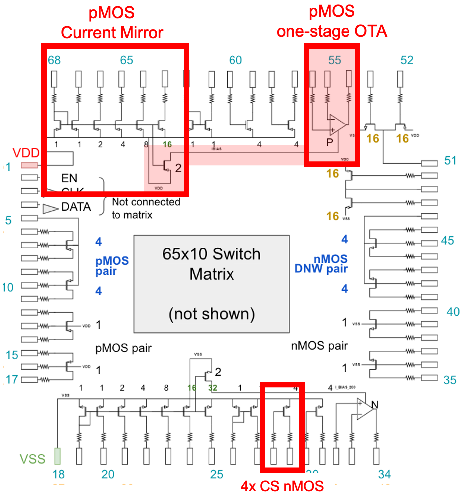
Fig. 3.10 Schematic of the MOSbius chip with one-stage pMOS OTA, the 4x CS transistor and the pMOS current mirror highlighted#
Materials#
MOSbius Chip & PCB
Breadboard & Wires
Resistors: \(100\Omega\) (two), \(100K\Omega\) (two)e
Signal Capacitors: \(470pF\), \(47nF\) and \(4.7nF\) or values that are close;
Bias Capacitors: \(47\mu F\) electrolytic and \(1\mu F\) non-electrolytic
Potentiometer: \(25K\Omega\)
ADALM2000 Active Learning Module (DC Power Supply, Oscilloscope, Waveform Generator, Network Analyzer)
Experiments#
The open-loop frequency response of the two-stage OTA is measured and compared with the expected response based on the behavioral models measured in One Stage OTA and Common-Source Amplifier Lab. The unity-gain step responses are reviewed. Then dominant-pole and Miller compensation are applied and the unity-gain step responses are reviewed again.
Two-Stage pMOS-input OTA without Compensation#
Build the Test Circuit and Check the Bias Point#

Fig. 3.11 Test circuit setup to measure the open-loop gain of the two-stage pMOS-input OTA. The input is a one-stage OTA biased with a 2x \(I_{REF}\) current bias; the second stage is a 4x CS nMOS transistor biased with a 4x \(I_{REF}\) current bias. The first and second stage are loaded by \(C_{L1}\) and \(C_{L2}\) respectively. The OTA is placed in negative DC feedback with \(R_2\), \(R_1\) and \(C_{B1}\) and in AC feedback with \(R_2\), \(R_1\). The biasing of the input pin is not shown.#
Build the test circuit:
The pMOS current mirror is biased using the 25K potentiometer provided on the PCB (close to I_REFP). Connect a current meter across I_REFP with the positive lead on the left and the negative lead on the right side of the header; adjust the potentiometer so \(I_{REF}\) is \(100\mu A\); replace the current meter with a jumper. The I_REFP header is connected to pin 68 of the MOSbius chip on the PCB. See Testing the Current Bias Potentiometers in the Appendix on Testing the MOSbius PCB
The OTA is internally connected to the current mirror with a 2X tail transistor M7 so it is biased with \(200\mu A\).
Use a \(470pF\) capacitor as \(C_{L1}\) and a \(4.7nF\) capacitor as \(C_{L12}\).
Use \(R_1 = 100\Omega\) and \(R_2 = 100K\Omega\) and \(C_{B1} = 1\mu F\) (non electrolytic).
Understand the operation of the OTA in the test circuit:
Draw a DC equivalent for the circuit and prove to yourself that the OTA is in negative, series-shunt feedback with unity gain for DC (\(\beta = 1\)).
Draw an AC equivalent for the circuit and prove to yourself that the OTA is in negative, series-shunt feedback with a feedback factor \(\beta\) of \(R_1/(R_1+R_2) = 1/1,001\) for AC signals.
Study for which frequencies the OTA will be in AC feedback, i.e. where \(\beta = R_1/(R_1+R_2)\).
What would happen if we connected \(R_1\) to \(V_{REF}\) directly instead of to \(C_{B1}\). (Hint: The OTA has a DC offset.)
Verify the DC bias point:
Set up your signal generator W1 to generate a constant \(1.25V\) reference.
Apply the 2.5V power supply to the chip and short in to W1.
Measure and record the various DC node voltages[1]: inn (= in), inp, OTAout, out.
Review that the voltages make sense.
If there is a voltage difference between out and inp, then likely there is leakage through \(C_{B1}\); make sure to use non-electrolytic (possibly smaller) capacitor.
Build and Characterize an Input-Signal Attenuator#
The signal generator is based on a DAC and it is difficult to generate small signals, say of a few milliVolt. Try it and you will notice that the signal looks like a staircase (after amplification) due to the generator’s DAC finite resolution.
Next we build an analog 100x attenuator so that we can use a large output signal from the generator but still apply the required small inputs for measuring an OTA with a lot of gain (40dB or more).

Fig. 3.12 Schematic of the 100x signal attenuator. It attenuates AC signals by 40dB while passing through DC bias.#
Build the attenuator circuit:
Use \(R_{atten1} = 10K\Omega\), \(R_{atten2} = 100\Omega\), and \(C_{Bin} = 10\mu F\)
Derive the transfer function for the attenuator across frequency.
How are DC signals handled by the attenuator circuit?
How are AC signals handled by the attenuator circuit?
For which signal frequencies does the circuit act as a 40dB attenuator?
Measure the attenuator circuit’s frequency response:
Use the network analyzer to characterize the frequency response of the attenuator.
Set up the network analyzer with a \(2V\) DC, \(V_{offset}\), and a \(1V_{p}\) signal, \(V_{signal}\).
Find the exact attenuation \(A_{atten}\), phase shift and frequency range of the attenuator for a close to \(40dB\) signal attenuation.
Explain what is happening at low frequencies. (Extra) Explain what is happening at high frequencies?
Oscilloscope Measurements#
We start with measurements on the oscilloscope at low frequencies to determine an appropriate input amplitude for the network analyzer measurements. We will also obtain a first estimate of the gains and these measurements can be used to do a sanity check on our network analyzer measurements later.
Gain:
Generate a \(1KHz\) \(200mV_{pp}\) sinewave with a \(1.25V\) DC offset with W1 and connect it to the attenuator. Always disconnect the signal generator first and verify the signal on the oscilloscope before applying it to your circuit. Do not apply signals above \(2.5V\) or below \(0V\) to the chip
Connect the attenuator output to the OTA input in.
Connect the oscilloscope channels 1+ and 2+ to W1 and out respectively and ground 1- and 2-.
Measure the waveforms at input and output and record the amplitudes.
Estimate the gain of the amplifier \(A=\frac{V_{out,pp}}{V_{in,pp}} + A_{atten}\).
Repeat with a \(100mV_{pp}\) and \(500mV_{pp}\) and check that the OTA operates in its linear range for an input of \(50mV_{pp}\).
Network Analyzer Measurements#
Gain vs Frequency:
Set up the Network Analyzer to use channel 1 as the reference and channel 2 as the output. Make sure to specify a signal with a 1.25V offset and \(100mV\) amplitude[2]. Turn on DC filtering at set the settling times to \(40ms\). Ten periods and 10 averages typically give good results. Turn on the scope view during NA measurements to verify the correct operation of the amplifier. Adjust the NA settings if needed.
Measure the \(A=\frac{V_{out}}{V_{in}} + A_{atten}\) between \(100Hz\) and \(1MHz\) using e.g. 200 points.
Can you determine the open-loop, LF gain of the two-stage OTA? What is an appropriate frequency to measure it?
Can you determine the frequency \(f_1\) of the dominant pole of the two-stage OTA’s open-loop frequency response?
Does the two-stage OTA have higher-order poles?
Check the slope of the frequency response.
What is the unity-gain frequency \(f_u\) of the two-stage OTA in open loop? Remember to correct for the effect of the input attenuator
Explain why you are measuring the open-loop performance of the OTA even though there is a feedback network around the OTA.
Measurement vs. Behavioral-Model Predictions#
Compare the measured frequency response of the two-stage OTA to the response you expected based on the behavioral model of the one-stage OTA and common-source amplifier measured in One Stage OTA and Common-Source Amplifier Lab.
Step Response Measurements#
Place the amplifier in unity-gain feedback. Directly out (pin 31) to inp (pin 56) of the one-stage OTA without any resistors or capacitors.
Generate a \(5kHz\) \(100mV_{pp}\) square wave with a \(1.25V\) offset. Connect in directly to the signal generator W1 without the attenuator.
Connect the oscilloscope channels 1+ and 2+ to W1 and out respectively and ground 1- and 2-.
Review the step response of the two-stage OTA.
Two-Stage pMOS-input OTA with Dominant-Pole Compensation#
Calculations#
Calculate the value of \(C_{L1}\) to do dominant pole compensation. Your goal is to make the unity-gain frequency of the loop-gain for a unity-gain feedback application equal to the frequency of the non-dominant pole created by the second stage and \(C_{L2}\).
Insert the new \(C_{L1}\) in the circuit.
Network Analyzer Measurements#
Put the two-stage OTA in the test circuit in Fig. 3.11 and measure the open-loop transfer function of the OTA. Remember to connect W1 through the input attenuator.
Check the position of the dominant pole and non-dominant pole. Assuming a unity-gain application (\(\beta=1\)), find the unity-gain frequency and the phase margin.
Do the measurements correspond to your calculations? Carefully review the magnitude and phase response of the open-loop gain.
Can you determine if there are additional poles or zeros in the circuit?
Step Response Measurements#
Put the two-stage OTA in unity-gain again and measure the step response.
Compare step responses with different input amplitudes[3]. Is the amplifier responding linearly?
Two-Stage pMOS-input OTA with Miller Compensation#
Calculations#
Replace \(C_{L1}\) with its original value of \(470pF\).
Calculate the value of the required Miller compensation capacitor \(C_M\) to obtain a phase margin of about \(45^o\) in a unity-gain (\(\beta = 1\)) application, i.e. \(f_{u,new} = f_{2,new}\)
Connect \(C_M\) between OTAout and out in the circuit.
Network Analyzer Measurements#
Put the two-stage OTA in the test circuit in Fig. 3.11 and measure the open-loop transfer function of the OTA. Remember to connect W1 through the input attenuator.
Check the position of the dominant pole and non-dominant pole. Assuming a unity-gain application (\(\beta=1\)), find the unity-gain frequency and the phase margin.
Do the measurements correspond to your calculations? Carefully review the magnitude and phase response of the open-loop gain.
Can you determine if there are additional poles or zeros in the circuit?
Step Response Measurements#
Put the two-stage OTA in unity-gain again and measure the step response.
Measure step responses with different input amplitudes[3]. Is the amplifier responding linearly?
RHP Zero Compensation#
Determine if you need to do compensation of the right-half plane zero due to \(C_M\) with a series resistor \(R_M\).
If yes, determine an appropriate value for \(R_M\) and insert it in the circuit.
Repeat the network analyzer measurements of the open-loop transfer function.
Repeat the measurement of the step responses.
Discuss the impact of placing the series resistor.
Dominant-Pole vs Miller Compensation#
Compare the amplifier’s performance as a unity-gain buffer when using dominant-pole vs Miller compensation.
Suggestions#
Run simulations of the experiments to gain insight in the circuit behavior. Note that simulations, measurements and calculations can differ due to the presence of parasitic capacitors on the chip and breadboard. However, we are using large capacitors in these experiments so that the effect of parasitic capacitors should be minimal.
Double the bias current on the one-stage OTA and the CS amplifier and observe the change in performance.
Try different compensation capacitor values to obtain higher phase margins and review the frequency response and step response.