1. MOSbius Platform for MOS Circuit Labs#
The MOSbius platform offers the MOSbius chip, an adapter PCB to place the chip on a solderless breadboard, and software tools to program the chip and process the measurement results. An LTspice library is also provided to run circuit simulations. The platform allows the (student) designer to experiment with and learn about MOS circuits in a uniquely hands-on environment.
1.1. MOSbius Chip#
1.1.1. Description#
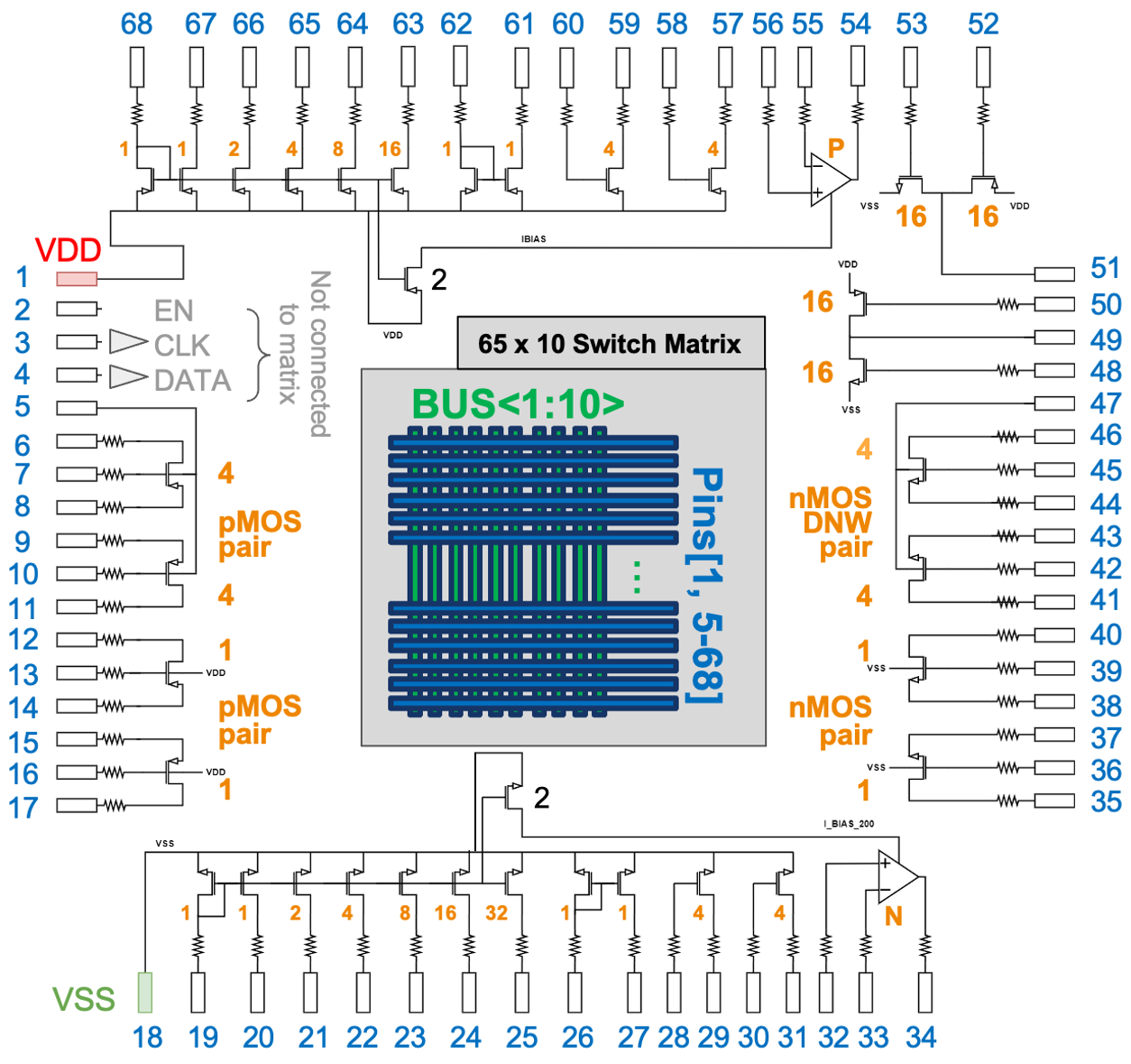
Fig. 1.1 Schematic of the MOSbius chip; pin numbers correspond to the numbering in the shift-register bitstream and the PCB labels#
The MOSbius chip is fabricated in a foundry 65nm CMOS technology and uses nMOS and pMOS thick-oxide transistors, i.e. the 2.5V I/O devices. It’s packaged in a 68-pin PLCC package.
The max. supply voltage \(V_{DD}\) is 2.5V. When the chip is in use, the supply should always be provided for ESD protection.
Device sizing: The ‘unit’ nMOS and pMOS have been sized to operate with an overdrive voltage \((V_{GS}-V_{TH})\) of 200mV for a drain-source current \(I_{DS}\) of 100\(\mu\)A.
The unit nMOS has a (W/L) of 16 and dimensions 8\(\mu\)m/0.5\(\mu\)m, laid out with 2 fingers
The unit pMOS has a (W/L) of 48 and dimensions 24\(\mu\)m/0.5\(\mu\)m, laid out with 6 fingers
These devices are marked as size 1 on the schematic; the sizes of other transistors are shown as multiples of the unit devices; they are laid out with the same finger size but the appropriate number of fingers.
Device configurations
nMOS
nMOS pair of size 1, with body connected to VSS
deep-nWell nMOS pair of size 4, with their common body terminal brought out to a pin
nMOS current mirrors
1 : 1, 2, 4, 8, 16, 32 nMOS current mirror with grounded sources and bodies
1 : 1 nMOS current mirror with grounded sources and bodies
nMOS common-source pair
common-source nMOS transistor pair of size 4 with grounded bodies
pMOS
pMOS pair of size 1, with body connected to VDD
nWell pMOS pair of size 4, with their common body terminal brought out to a pin
pMOS current mirrors
1 : 1, 2, 4, 8, 16 pMOS current mirror with sources and bodies connected to VDD
1 : 1 pMOS current mirror with sources and bodies connected to VDD
pMOS common-source pair
common-source pMOS transistor pair of size 4 with bodies connected to VDD
Operational Transconductance Amplifiers (OTAs)
one-stage, nMOS-input, load-compensated OTA
one-stage, pMOS-input, load-compensated OTA
The OTAs are biased through the current mirror with a 2x device
nMOS/pMOS stacks
two nMOS/pMOS stacked devices of size 16
The
ENpinThe pin is pulled down to \(V_{SS}\) with an internal pull-down resistor.
When
ENis LOW, the on-chip switch matrix disabled; the chip can be used without digitally programming the switch matrix.
The pin can be externally pulled up to \(V_{DD}\) to enable the switch matrix (see below).
When
ENis HIGH, the on-chip switch matrix connects devices according to the bit pattern streamed into the on-chip memory through the digital serial interface.
ESD series resistors
To meet ESD requirements series resistors have been inserted between the device terminals and the chip pads; the resistor size depends on the transistor size: 50\(\Omega\) for the 1x device, 25\(\Omega\) for the 1x device, and 12.5\(\Omega\) for the 4x and larger devices.
1.1.2. On-Chip Switch Matrix#
The chip can be used without using the switch matrix; if the
ENsignal is left disconnected[1] or kept LOW, all switches remain open. All devices are hardwired to the chip pins and circuits can be constructed using external connections.Switch matrix and buses
There is a 65x10 switch matrix than can connect each of the 63 transistor-terminal pins and the VDD and VSS to 10 buses on the chip to build circuits without requiring external wiring.
Through the serial interface pins
DATAandCLKa digital bit stream can be read into the on-chip memory whileENis LOW; after assertingENto HIGH, the respective 15\(\Omega\) transmission-gate switches are activated.
The chip can be programmed using the MOSbiusTools.
1.2. MOSbius Test PCB#
1.2.1. Description#
The MOSbius PCB is a ‘breakout’ board that allows to connect the chip to a standard solderless breadboard. All the pins of the chip are routed to pins on the breadboard so that external connections and external components can be connected to the circuit.
Schematic and PCB Silk/Labels, PCB Top Wires, PCB Bottom Wires
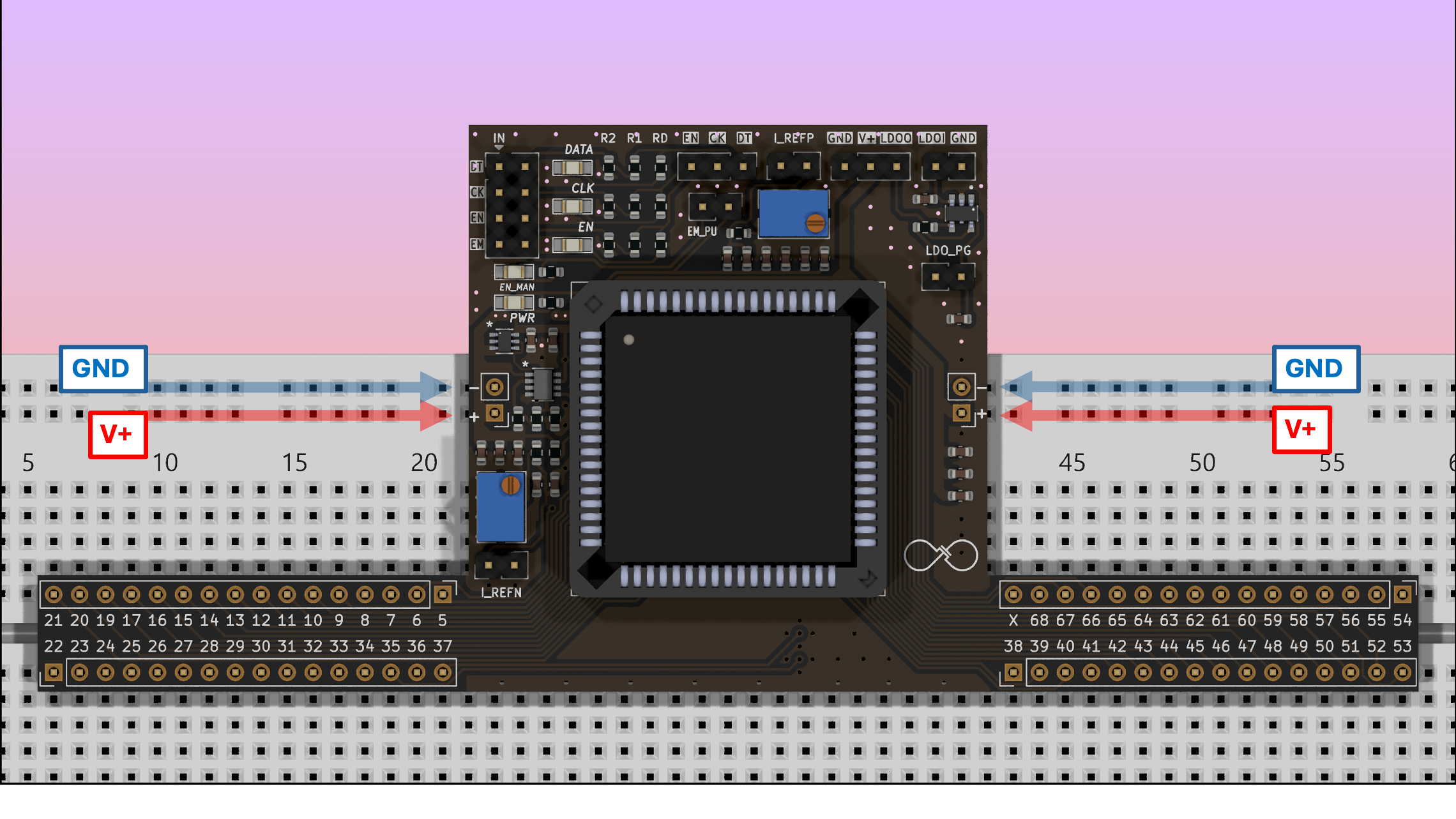
Fig. 1.2 3D Render of the MOSbius chip on the MOSbius break-out PCB inserted in a solderless breadboard.#
1.2.2. Testing the PCB Before Use#
Testing the PCB has images showing the various functions on the PCB.
1.2.3. Using the PCB#
Power Supply:
The MOSbius chip always needs to be powered by 2.5V to reverse bias the pad ESD protection diodes. All
GNDon the PCB are connected, but make sure to connect it correctly to your external power supply.You can apply a 2.5V supply to the
V+pin on the top of the PCB; the PCB contains a protection circuit against supply voltages larger than 2.5V. The power supply is connected to the breadboard power rails as well. The 2.5V supply can be supplied from there also.Or you can use the LDO regulator[2] on the PCB to convert an input voltage
LDOIbetween 2.7V and 5.5V to 2.5V. In that case place a jumper betweenLDOOandV+. You can obtain the ‘Power Good’ logic signal with a jumper onLDO_PGand measuring the voltage, but this is not required.The red power LED indicates that 2.5V is applied to the chip. The PCB also contains supply decoupling.
nMOS and pMOS Current Mirror Bias:
The 25K potentiometer on the top, close to
I_REFPcan be used to bias the pMOS current mirror. Connect a current meter acrossI_REFPwith the positive lead on the left and the negative lead on the right side of the header; adjust the potentiometer for the desired current and then replace the current meter with a jumper. The left terminal of theI_REFPheader is connected topin 68of the Mobius chip.Similarly, the 25K potentiometer on the left, close to
I_REFNcan be used to bias the nMOS current mirror. Connect a current meter acrossI_REFNwith the positive lead on the left and the negative lead on the right side of the header; adjust the potentiometer for the desired current and then replace the current meter with a jumper. The left terminal of theI_REFNheader is connected topin 19of the Mobius chip.
Digital Interface Level Conversion:
The PCB contains resistive dividers to convert 3.3V logic signals to 2.5V logic signals compatible with the MOSbius chip.
Connect the
DATA,CLK, andENfrom your 3.3V digital signal source to the respective headersDT,CKandENon the top of the PCB.The 2.5V logic signals will appear on the right side on of the header in the upper left corner of the PCB. Place a jumper to connect the
DT,CKandENto the chip. The left side of the header is connected to the MOSbius chippins 3, 2, 1respectively.The blue, yellow and green LED’s will light up when you send the digital
DT,CLKandENsignals to the chip: .
Manual Enable:
If you want to control
ENmanually, then connect a jumper to connectEMto the chip; if you then connect a jumper atEM_PU,ENat the chip will go high enabling the switch matrix and the orange LED will light up; if you leave theEM_PUjumper open,ENat the chip will stay low and the on-chip switches in the switch matrix will remain open.
1.3. Testbench#
The MOSbius chip can be measured using standard test equipment on a typical student lab bench.
We recommend the use of USB-based instrumentation since it allows the student to do the experiments in their dorm room or at home. For many of the experiment demonstrations shown here we use the ADALM 2000 Active Learning Module, but other modules can be used as well.