2.2. A ‘555’ with MOSbius#
2.2.1. Background#
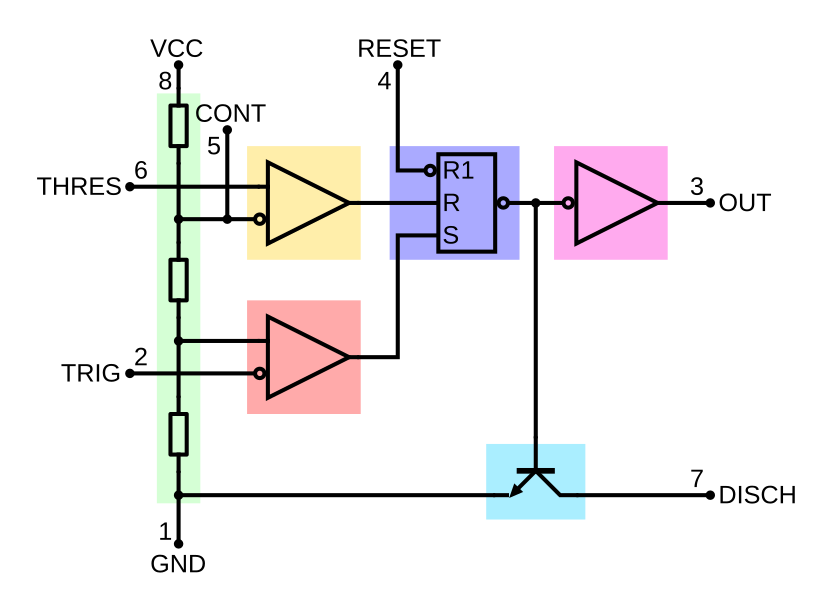
The ‘555’ is an iconic chip that is often used in entry-level electronic experiments. This Wikipedia article has a detailed description. The original Signetics NE555 was a bipolar design, and later CMOS versions became available. The MOSbius chip has the necessary devices to create the 555 functionality. It offers an opportunity not only to build 555 projects, but dig into the internal operation of the 555 chip.
2.2.2. Building a 555 with MOSbius#
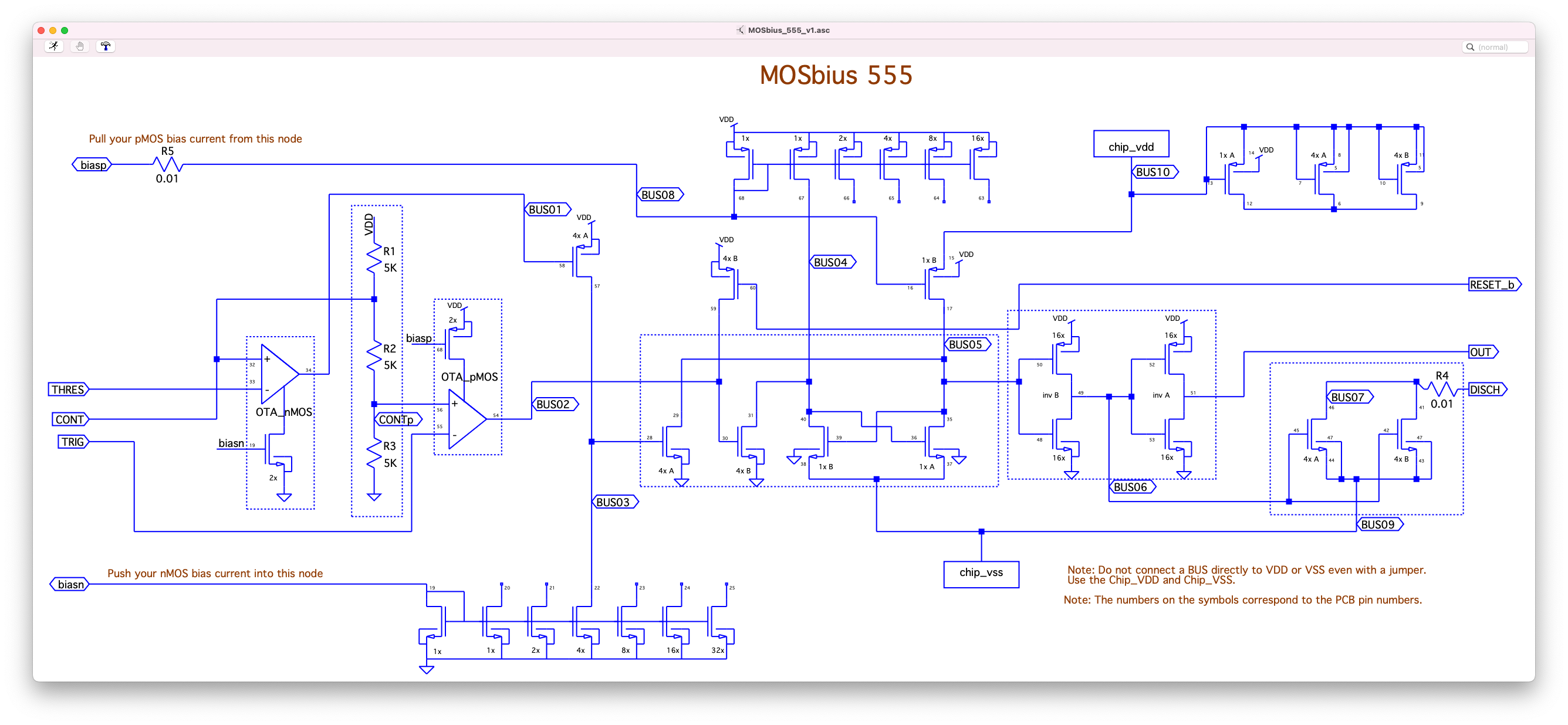
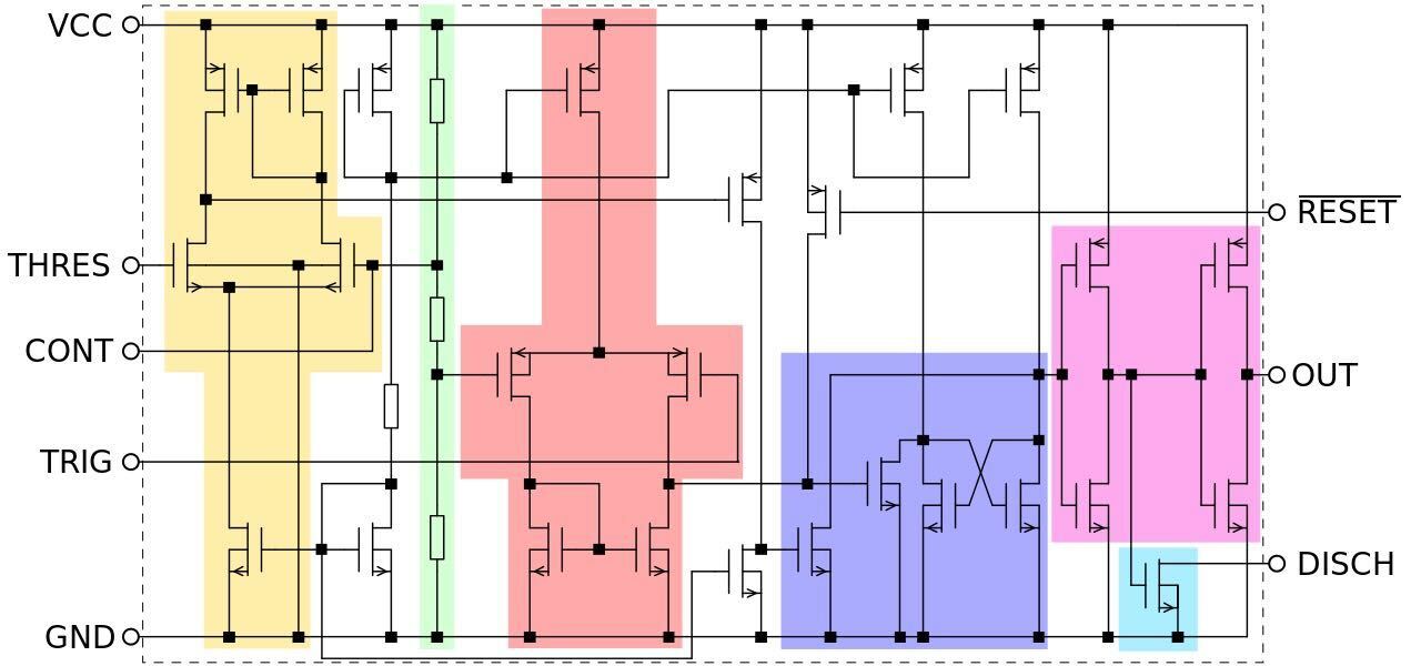
Fig. 2.12 Schematic for the MOSbius 555 implementation#
The 555 MOS schematic[1] can be implemented in a straightforward manner. Care must be taken to use the correct sizes for various devices depending on their function. In this realization the S/R latch is implemented with 1x devices with the set and reset devices realized with 4x nMOS transistors. For the output inverters the 16x inverter pairs are used for good driving strength on OUT, however, they load the S/R latch output (bus05). All connections can be realized with the on-chip buses (connections file) and the reference ladder (R1-R2-R3) is realized with off-chip 5K-5K-5K resistors. The terminals biasn (pin 19) and biasp (pin 68) are biased with 100\(\mu A\) using the potentiometers on the PCB to bias the OTA-nMOS and OTA_pMOS blocks and some additional current source devices.
2.2.3. Building a Timer with the MOSbius 555 in Astable Mode#
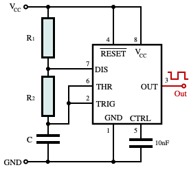
Fig. 2.13 Timer with the 555 operating in astable mode#
The timer using the 555 in astable mode can easily be implemented using the MOSbius 555.
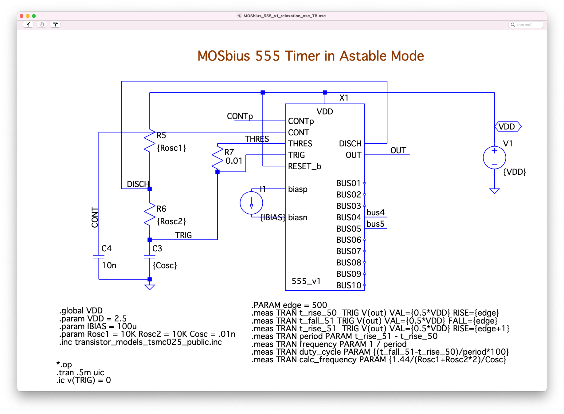
Fig. 2.14 Simulation schematic for a timer built with the MOSbius 555 operating in astable mode#
2.2.4. Measured Results#
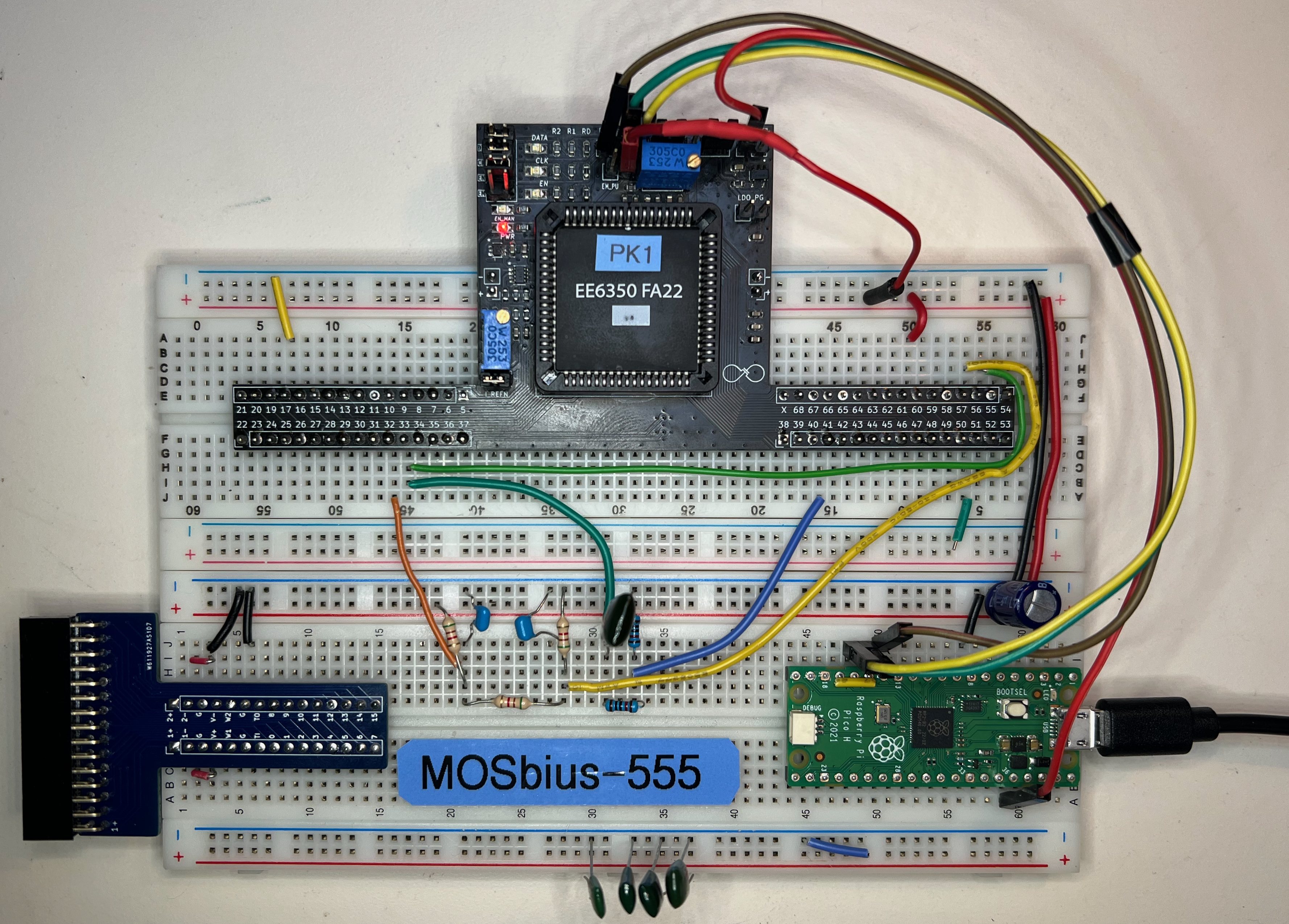
Fig. 2.15 Picture of the test setup of the timer built with the MOSbius 555 operating in astable mode; the 5K-5K-5K ladder is above the blue label; the Raspberry Pi PICO microcontroller in the lower right corner programs the switch matrix on the MOSbius chip.#
We built the timer and evaluated the performance for different frequencies of operation. The R1/Rosc1 and R2/Rosc2 resistors were set to 10K\(\Omega\) and the capacitor value was changed; the frequency was measured on the OUT node while no other probes where attached to avoid additional loading.
Cap [nF] |
\(f_{calc}\) [kHz] |
\(f_{meas}\) [kHz] |
Error [%] |
|---|---|---|---|
57.9 |
0.821 |
0.807 |
1.7 |
22.0 |
2.160 |
2.120 |
1.9 |
10.3 |
4.614 |
4.320 |
6.4 |
5.66 |
8.397 |
7.580 |
9.7 |
0.976 |
48.690 |
33.700 |
30.7 |
0 |
241 |
When operating up to a few kHz the frequency of operation is close to the value predicted based on the properties of the RC network: \(f_{calc} = \frac{1}{\ln(2)(R_1 + 2 R_2) C}\) [Wikipedia]; we measured the actual resistor values (measured 10.1K\(\Omega\)) and capacitor values (see table) for the frequency calculation. The measured frequency is systematically lower due to the additional propagation delay through the 555.
Waveforms: f = 2.16kHz C = 22nF#
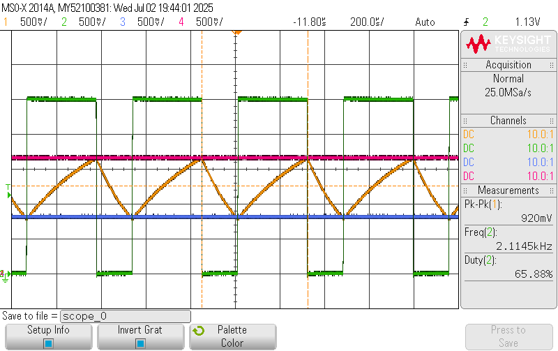
Fig. 2.16 Waveforms for C=22nF with TRIG/THRES, OUT, CONT, and CONTp on channels 1 thru 4 respectively; due the loading by the 1:10 probes, the frequency is slightly lower then when only OUT is observed.#
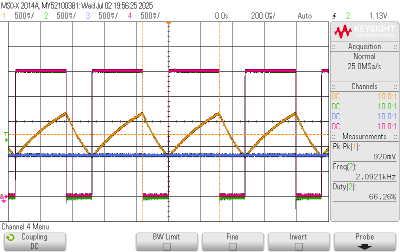
Fig. 2.17 Measured waveforms for TRIG/THRES, OUT, CONTp, and the internal S/R latch output (bus05) on channels 1 through 4 respectively for C=22nF.#
When the capacitor voltage (CH1, yellow) reaches the 1/3 VDD reference (CH3, blue), bus05 (CH4, red) and the output waveform (CH2, green) switch almost instantaneously. The 555 circuit does not add significant delay and the oscillation frequency is very close to the frequency predicted by the values of the R-C network.
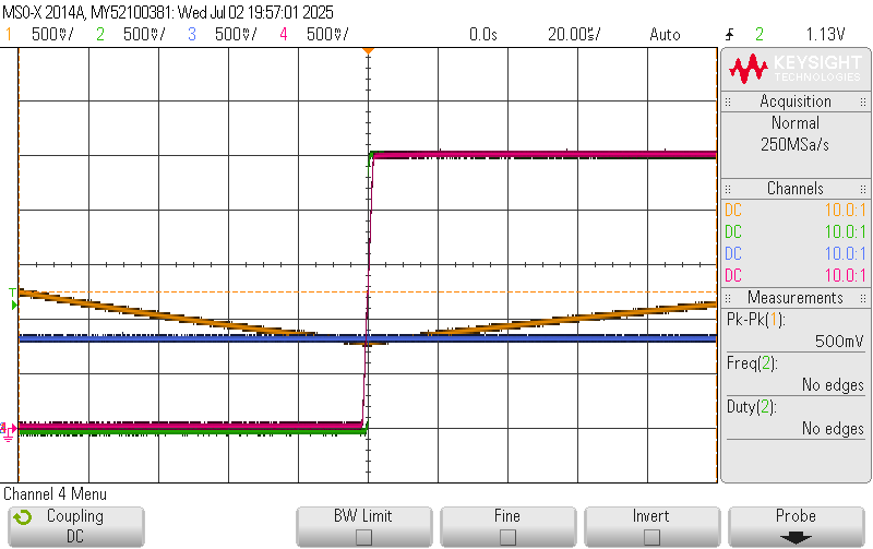
Fig. 2.18 Zooming in on the measured waveforms for TRIG/THRES, OUT, CONTp, and the internal S/R latch output (bus05) close to the transition; the delay between TRIG/THRES reaching CONTp and the S/R latch and OUT switching is very small relative to the period.#
Waveforms: f = 48.7kHz C = 1nF#
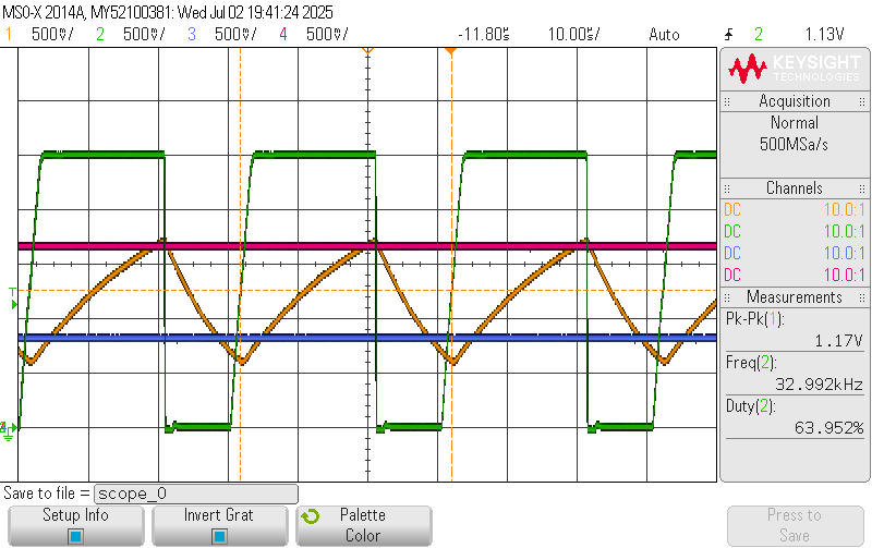
Fig. 2.19 Waveforms for C=1nF with TRIG/THRES, OUT, CONT, and CONTp on channels 1 thru 4 respectively; due to the propagation delay there is a slight overshoot on the capacitor voltage (TRIG/THRES) beyond CONT, and a significant undershoot below CONTp.#
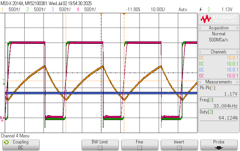
Fig. 2.20 Measured waveforms for TRIG/THRES, OUT, CONTp, and the internal signal bus05 on channels 1 through 4 respectively for C=1nF.#
The capacitor voltage (CH1, yellow) goes below the 1/3 VDD reference (CH3, blue) because the S/R latch output’s (bus05) rise time is relatively large compared to the period, adding delay, which delays the switching of the output and the start of the discharge; hence, the undershoot on the capacitor voltage (CH1, yellow). The delay added by the 555 circuit reduces the oscillation frequency significantly.
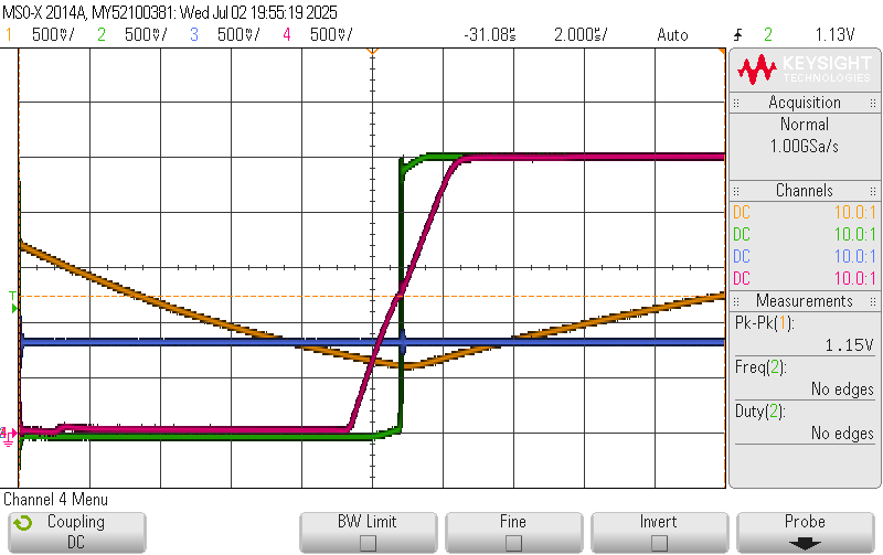
Fig. 2.21 Zooming in on the measured waveforms for TRIG/THRES, OUT, CONTp, and and the internal S/R latch output (bus05) close to the transition; the delay between TRIG/THRES reaching CONTp and the S/R latch output and OUT switching is quite significant compared to the period.#
Waveforms: f = 241kHz C = 0nF#
Note that when no capacitor is placed, the oscillation frequency goes to 241kHz but the waveforms look very different. As observed before in the current implementation the S/R latch output struggles to drive the output inverters when going high.
But this experiment offers an indication of the absolute max. frequency this circuit can support. Practical uses with frequencies defined by the passive components will need to be significantly below 100kHz as the measured results in the table prove.
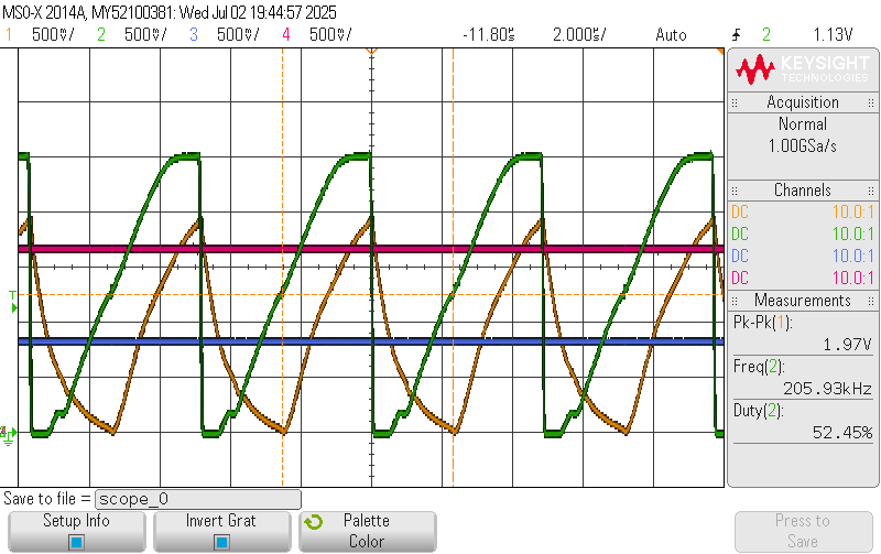
Fig. 2.22 Waveforms when no external capacitor is used TRIG/THRES, OUT, CONT, and CONTp are on channels 1 thru 4 respectively; due the loading by the 1:10 probes, the frequency is lower then when only OUT is observed.#
2.2.5. Next Steps#
Learners can now look for alternate implementations of the 555 functionality with MOSbius to get faster performance.