Automated pMOS I-V Data vs Simulations#
Caveat: This is a preliminary example to illustrate the opportunity of measuring I-V characteristics. Some comparison is included to the simulated results, but given an public-domain model card is used that is not really optimized for this technology, the matching is not expected to be very good. Some basic analysis was done to try to make simulations match measurements, but it is very limited and incomplete.
pMOS 1x Diode-Connected Devices#
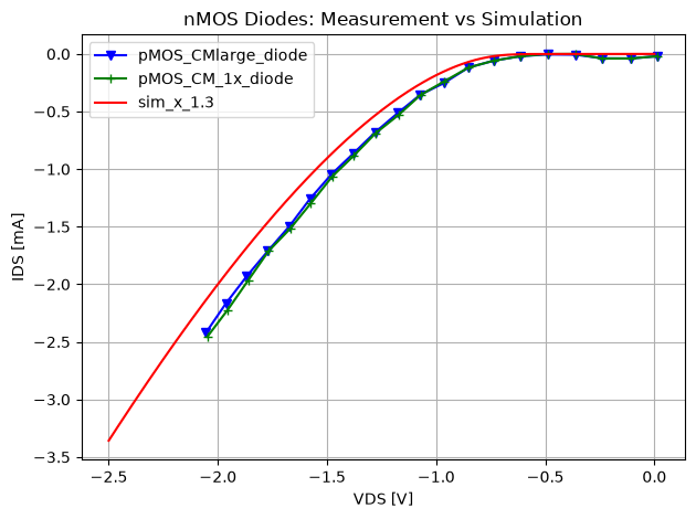
There are two diode connected pMOS devices on the chip as part of the current mirrors. We first measure their IDS-VGS characteristics.
Collecting the Simulation Data#
Collecting the Measurement Data#
dict_keys(['pMOS_CMlarge_diode', 'pMOS_CM_1x_diode'])
IDS-VGS Measurement vs Simulation#
model_scaling = 1.30
Observations:
The transistors are diode connected so VDS=VGS.
We get a fairly good correspondence between simulation and measurement if we scale the simulation data up.
This seems to indicate that the mobility is higher on the chip than in the simulation and/or the threshold voltage lower; remember that the model used is a public domain model, not even optimized for this technology.
pMOS Current-Mirror Devices#
Here we evaluate the nMOS current mirror, specifically the 1x, 2x, 4x, 8x and 16x devices.
Collecting the Simulation Data#
[0.75, 1, 1.25, 1.5, 1.75, 2, 2.25]
Collecting the Measurement Data#
dict_keys(['pMOS_CMlarge_1x', 'pMOS_CMlarge_2x', 'pMOS_CMlarge_4x', 'pMOS_CMlarge_8x', 'pMOS_CMlarge_16x'])
model_scaling = 1.30
IDS-VDS Measurement vs Simulation#
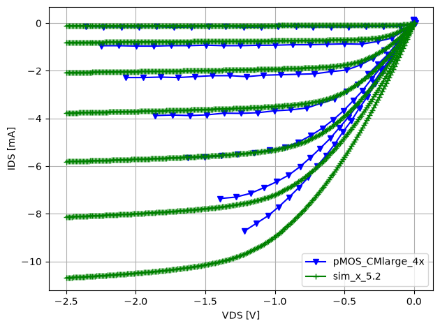
colors = itertools.cycle(['b', 'g', 'r', 'c', 'm', 'y', 'k'])
markers = itertools.cycle(('v', '+', '.', 'o', '*', "s"))

sim_scaling = model_scaling * 8
name = list(data_collection.keys())[3]
fig, ax = plt.subplots()
plot_data(ax, data_collection[name], color=next(colors), marker=next(markers)+'-', name=name, R_meas=94/100)
plot_data(ax, sim_cm_data['1x'], color=next(colors), marker=next(markers)+'-', name=f'sim_x_{sim_scaling}', R_meas=1/sim_scaling)
# ax.get_legend().remove()
fig.tight_layout()
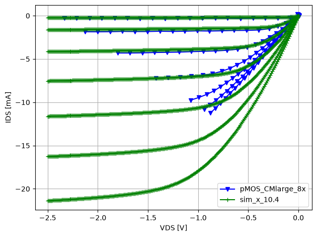
Observations:
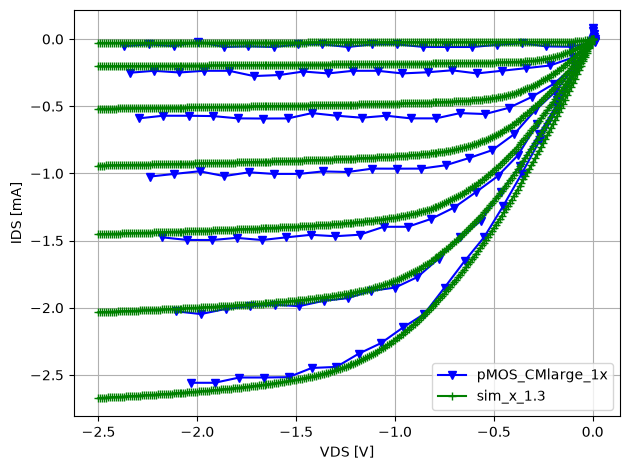
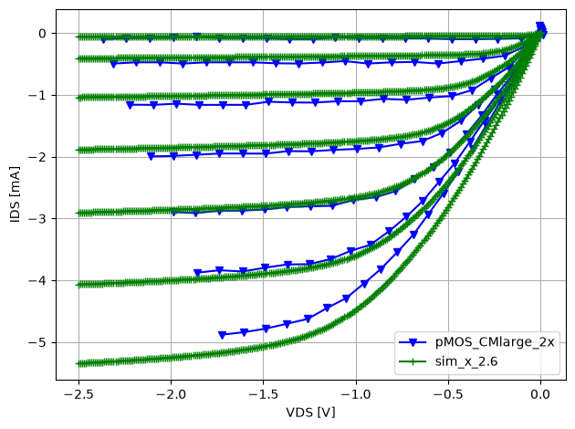
The correspondence between measurement and simulation in saturation is remarkably good when the simulation data is scaled up by 30%, especially considering that the public-domain model used is not optimized for this techology.
The fit in the linear region is less good and reviewed further below.
Current Mirror Scaling#
In an ideal current mirror the IDS-VDS characteristic scales with the mirror factor. here we plot the ‘normalized’ currents, so e.g. for the 8x device we plot IDS/8, and so on. To the first order, the characteristics should overlap. (In the layout good practices were applied to get accurate current mirror factors.)
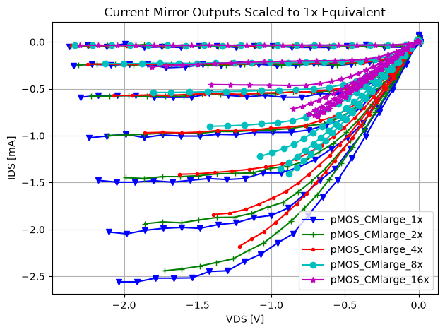
Observations:
In saturation the overlap is very good, especially given the limited accuracy of our setup.
In the linear region the smaller transistor sizes overlap but the larger transistors do not.
Looking at Parasitic Resistance#
In the linear region, especially for the larger devices, the IDS-VDS characteristic measurement is sensitive to possible series resistance since the \(R_{ds}\) of the devices becomes small. We notice that as the VSG increases (and thus the \(R_{ds}\) reduces), the |IDS| does not increase in the linear region, seeming to indicate the presence of a parasitic series resistor. Here we estimate the value of those resistors.
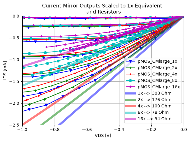
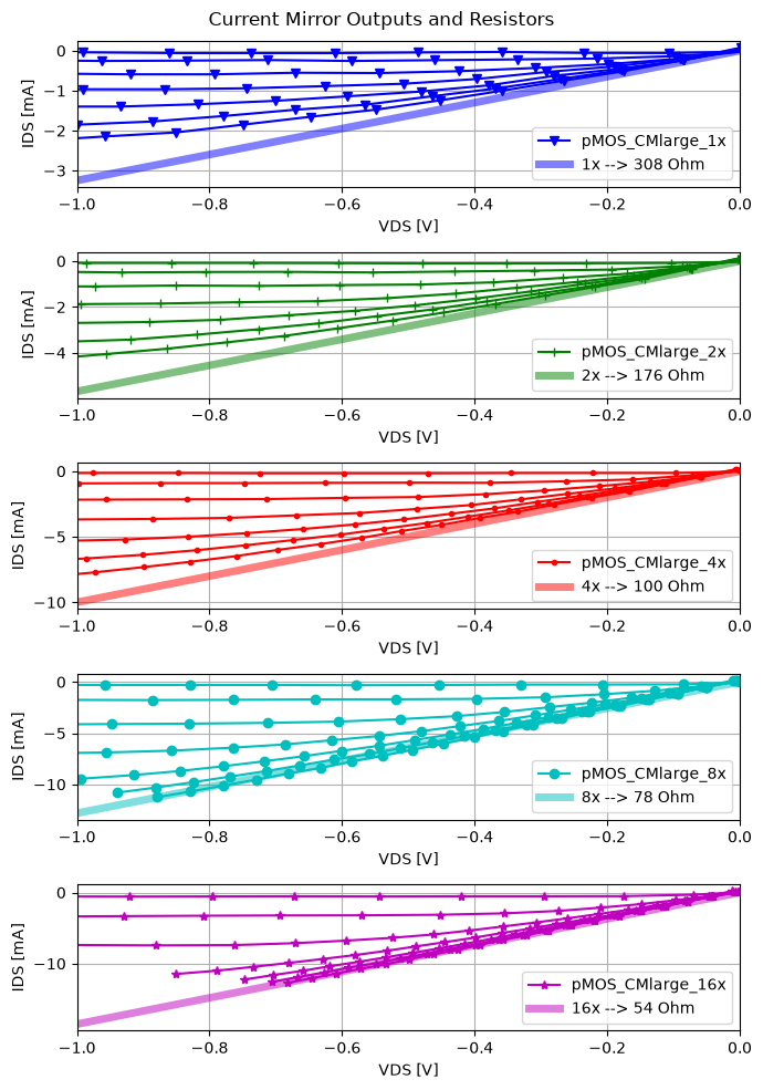
Observations:
There are series resistors placed for ESD reasons on the pins (e.g. \(\approx 12.5\Omega\) for the 8x device, see chip description), but they were nominally designed to be smaller than the values found here.
Possibly additional routing parasitics or measurement parasitics play a role here.