2.3.1. Two-Stage Miller-Compensated OTA with pMOS Input Stage#
Caveat: This section is a work in progress. Many of the measurements presented here are relatively straightforward configurations. There are various methods to measure offset, DC gain, frequency response, noise, linearity, … and it will be instructive to the student to explore some of these techniques. At this stage, we are often starting with simpler measurements not to overwhelm the student and to build some appreciation of the challenges involved in experimental characterization.
Schematic Design and Operating Point#
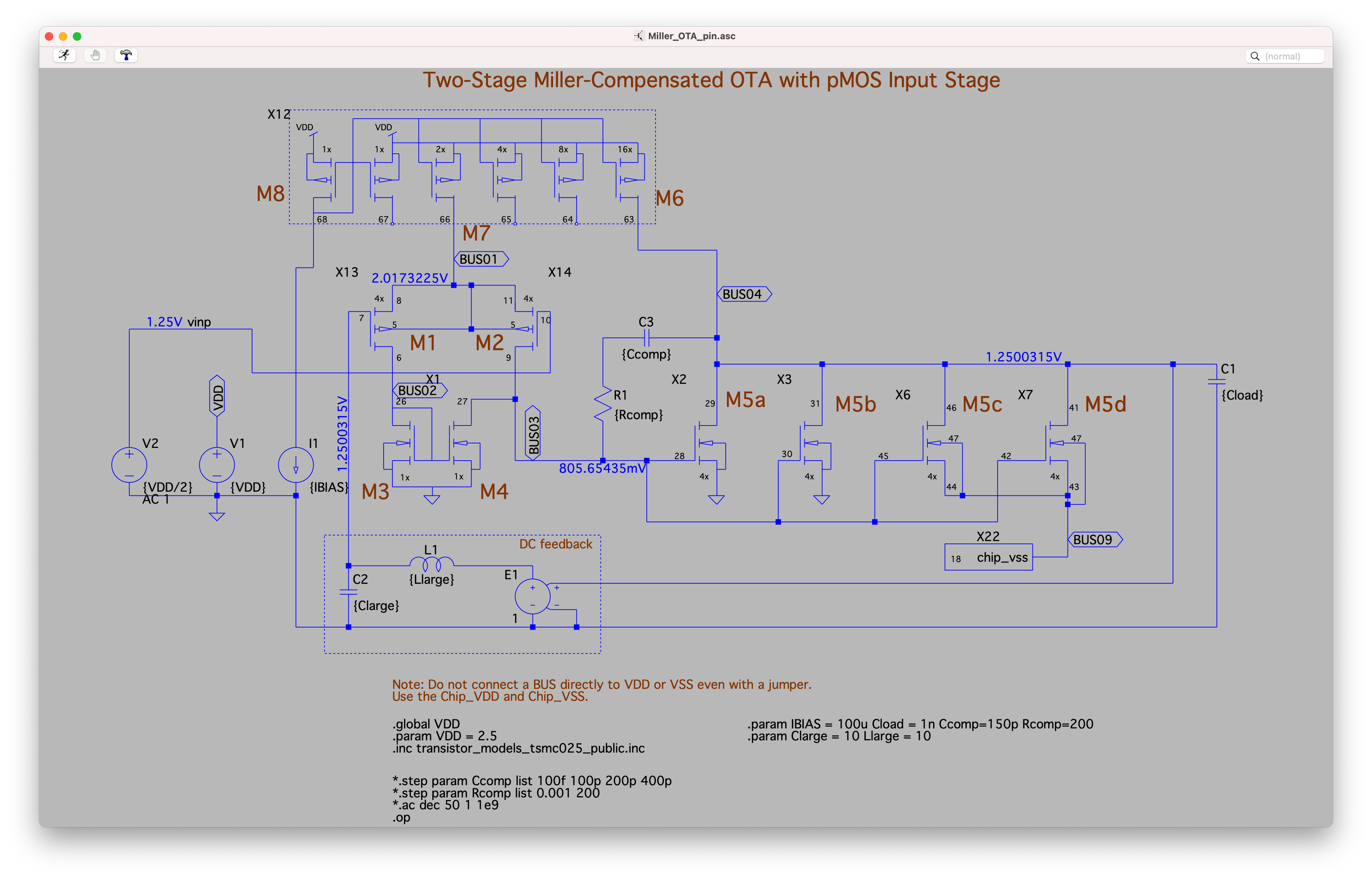
Fig. 2.13 Simulation schematic of the two-stage Miller-compensated OTA including an external DC feedback for open-loop AC simulations#
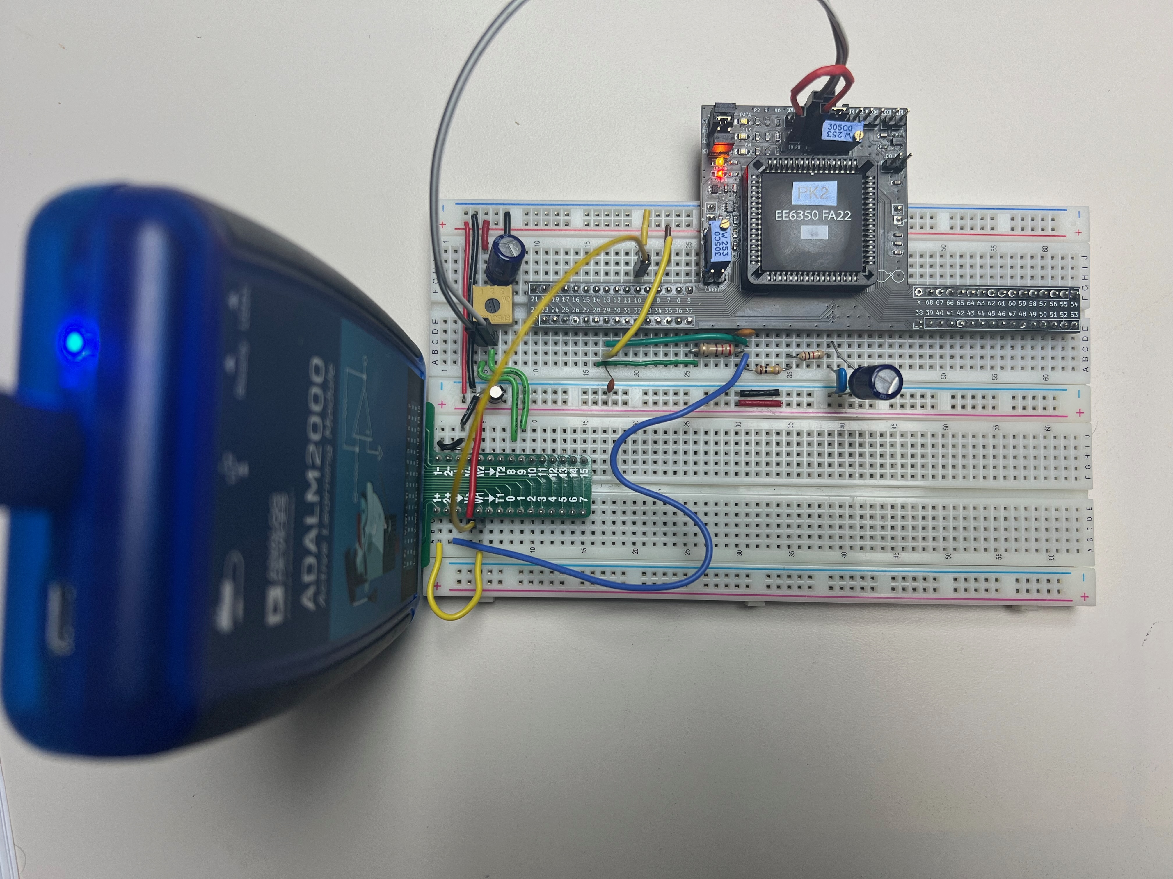
Fig. 2.14 Solderless breadboard setup for the two-stage Miller-compensated OTA configured in unity-gain feedback#
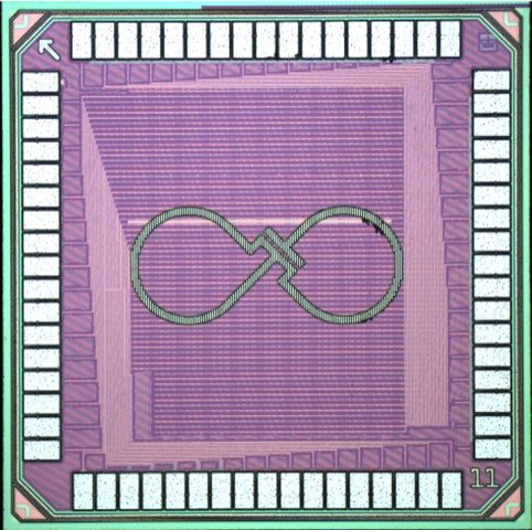
A two-stage Miller-Compensated OTA with a 4x pMOS input differential pair and a 16x nMOS second stage is biased with a nominal 1x current of 100uA. Files:(<TBD spice lib> cir, bitstream, clk_bitstream)
The operating point of the transistors is obtained from an LTSpice simulation[1]:
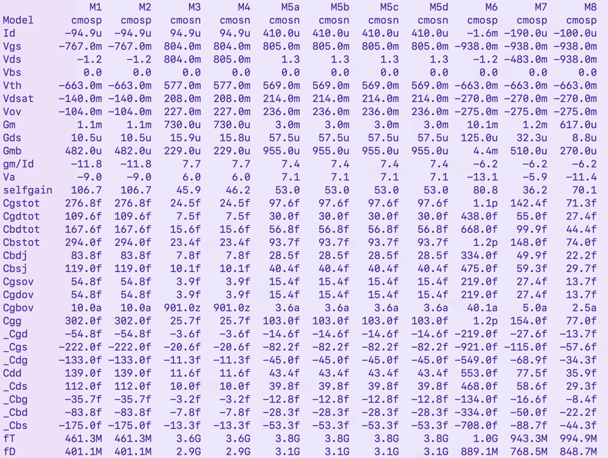
Fig. 2.15 Simulated DC operating point#
The pMOS input pair M1/M2 are biased towards weak inversion with a \((g_m/I)\) of ~12 and a \(g_{m,1}\) of 1.1mS; the second stage M5 is biased in strong inversion with a \((g_m/I)\) of ~7 and a \(g_{m,5}\) of 12mS.
Here is an overview of the OTA design:
parameter |
expression |
value |
|---|---|---|
\(C_L\) |
1nF |
|
\(C_{comp}\) |
150pF |
|
\(R_{comp}\) |
200\(\Omega\) |
|
\(f_u\) |
\(g_{m,1}/(2\pi C_{comp})\) |
1.16MHz |
\(f_2\) |
\(g_{m,5}/(2\pi C_{L})\) |
1.91MHz |
\(f_z\) |
\(g_{m,5}/(2\pi C_{comp})\) |
12.73 MHz |
We connect the \(C_L\) between the output (BUS04) VSS (multiple pins can be chosen in the attached picture we used pin 29) and connect the series combination of \(R_{comp}\) and \(C_{comp}\) between the output (BUS04, pin29) and the input of the second stage (BUS03, pin28).
Unity-Gain Configuration#
We start of by putting the OTA in a unity gain configuration by connecting the output (BUS04, pin 29) to the negative input (pin 7).
DC Ranges#
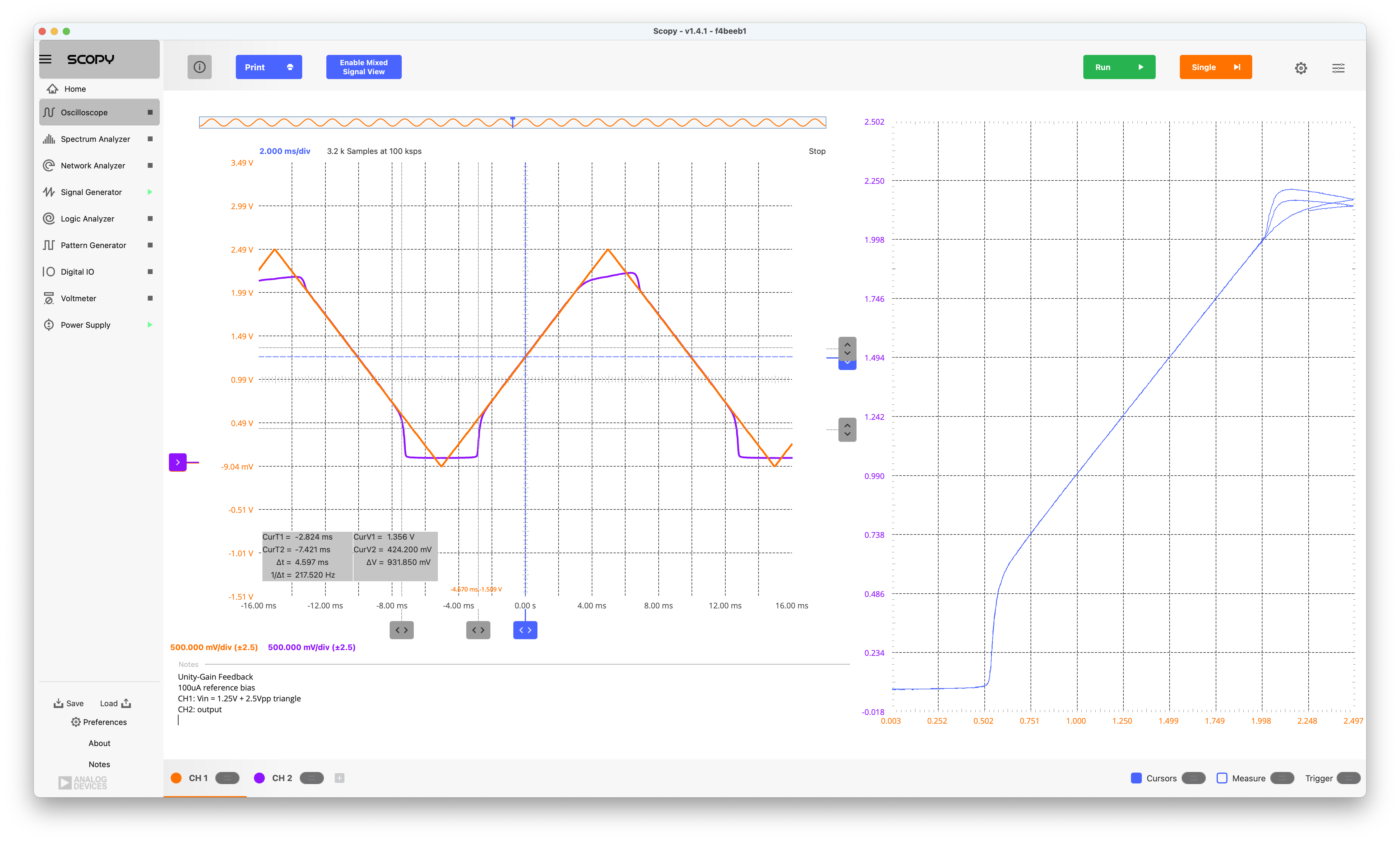
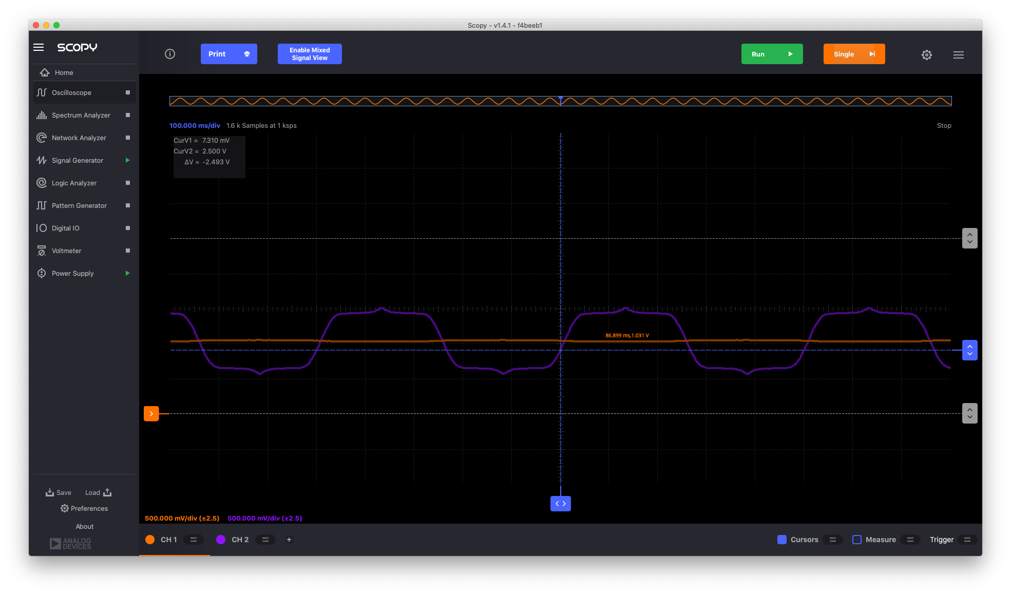
Fig. 2.16 The measured DC transfer characteristic of the OTA in unity-gain feedback (XY-plot, right) measured using a sawtooth input (left)#
Applying a rail-to-rail, low-frequency, sawtooth waveform to the positive input allows the measurement of the signal ranges. The output follows the input for inputs between about 0.57V and 2V
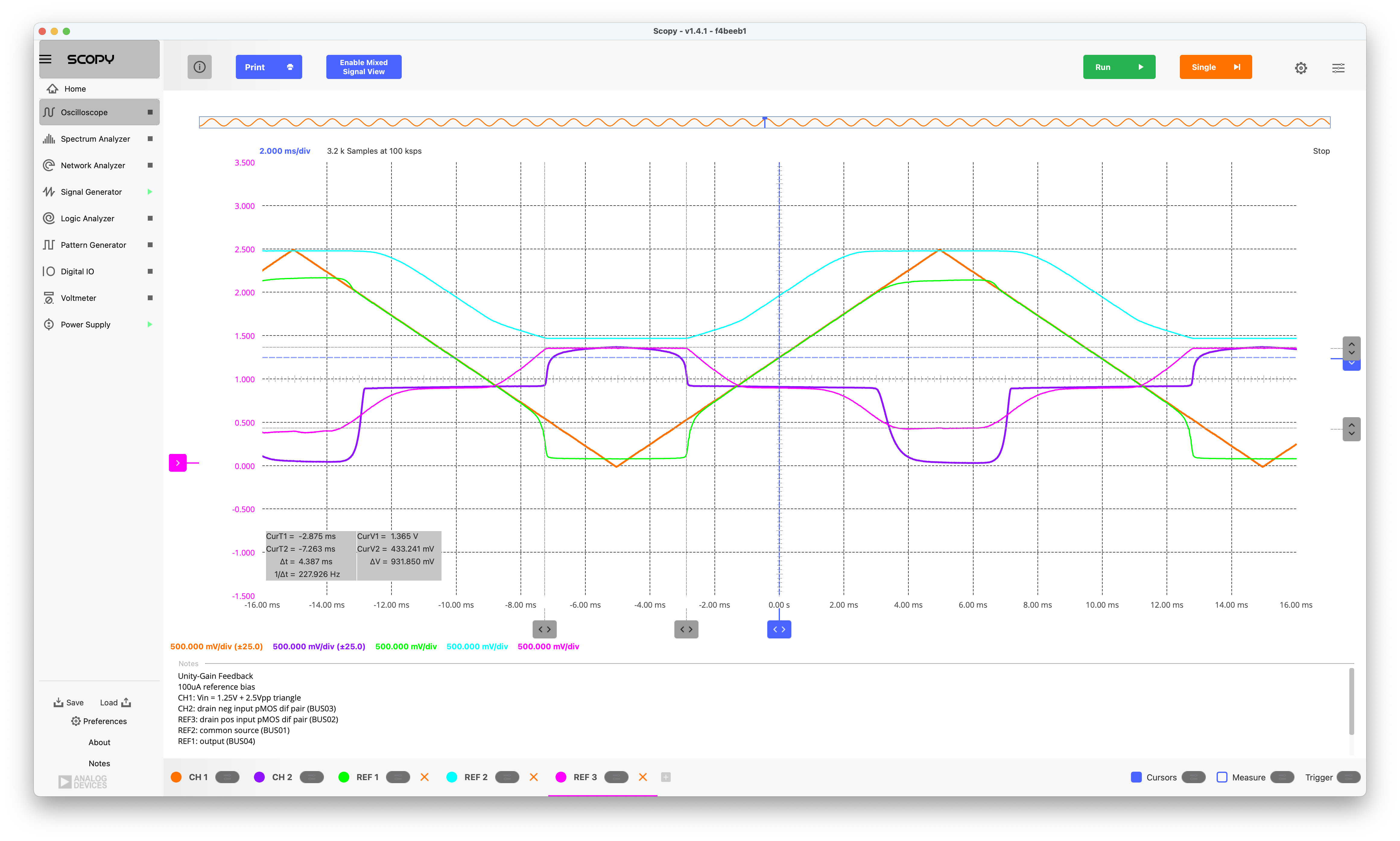
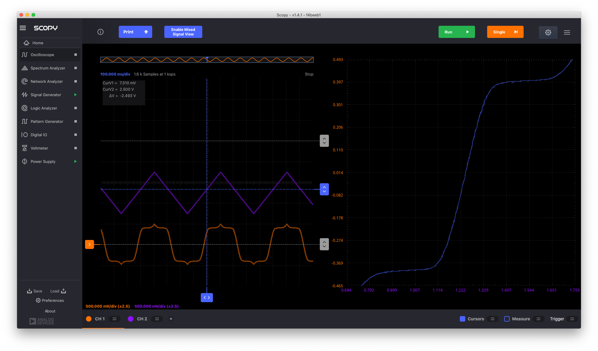
Fig. 2.17 Measurement of all internal OTA nodes for a rail-to-rail input signal; CH1 was kept on the input, while CH2 was moved to different nodes and ‘snapshots’ were taken and saved.#
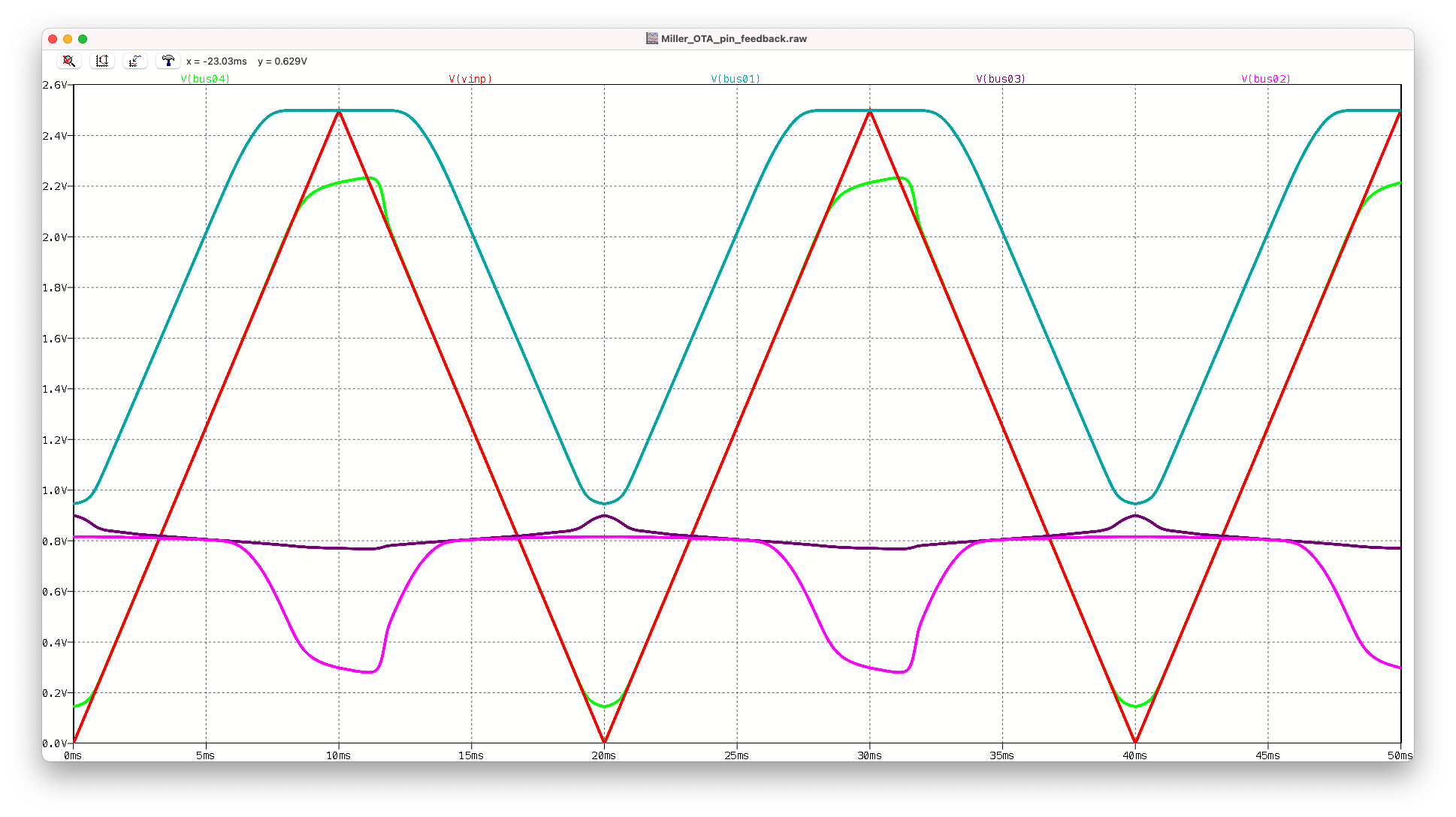
Fig. 2.18 Simulated internal nodes of the OTA with a rail-to-rail input signal#
Measured and simulated internal voltage nodes are qualitatively similar to some extent but there are important differences. The output (BUS04), BUS02, and BUS03 behavior are quite different for low input voltages; the BUS03 behavior for high input voltages are also quite different. For an input of 1.25V, the correspondence between measurement and simulation is very good. The differences warrant further investigations; they could be due to limited modeling accuracy of the simulated circuits given that in the experimental device all nodes are connected off-chip. This introduces additional parasitics (pads, pins, ESD) and the measurement equipment also introduces additional loading.
Gain and Offset from DC Sweep#
Taking the Vout-Vin data measured with the sawtooth input into a jupyter notebook and performing linear regression using the scipy.stats.linregress function, we get the following fits:
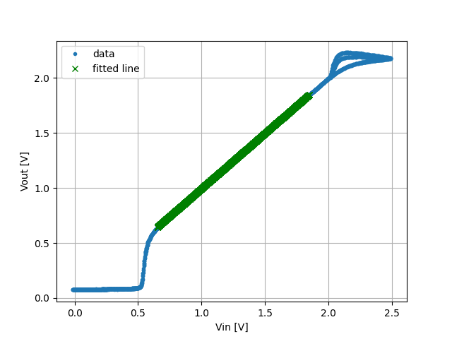
Fig. 2.19 Input-Output characteristic of the unity-gain buffer with a linear fit for Vin \(\in\) [0.65, 1.85]#
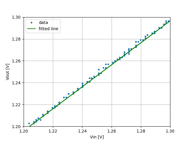
Fig. 2.20 Zoom in for the input-output characteristic and linear fit#
We then run the fitting for different input voltage ranges:
1.15 < Vin < 1.35
Linear Regression: Vout = -0.0083 + 1.0046 Vin
Linear Regression: Vout = 1.0046 (Vin + -0.0083)

1.05 < Vin < 1.45
Linear Regression: Vout = -0.0025 + 1.0000 Vin
Linear Regression: Vout = 1.0000 (Vin + -0.0025)

0.95 < Vin < 1.55
Linear Regression: Vout = -0.0023 + 0.9999 Vin
Linear Regression: Vout = 0.9999 (Vin + -0.0023)

0.85 < Vin < 1.65
Linear Regression: Vout = -0.0034 + 1.0006 Vin
Linear Regression: Vout = 1.0006 (Vin + -0.0034)

0.75 < Vin < 1.75
Linear Regression: Vout = -0.0062 + 1.0025 Vin
Linear Regression: Vout = 1.0025 (Vin + -0.0062)

0.65 < Vin < 1.85
Linear Regression: Vout = -0.0105 + 1.0054 Vin
Linear Regression: Vout = 1.0054 (Vin + -0.0104)
Ideally small changes of the Vin range should not affect the fitting results, especially in the middle of the range; however, due to measurement accuracy limitations we see variations in the offset estimation at the mV level and in the gain estimation below the 1% level. We can conclude that the transfer curve has a gain which is close to 1.00 and an negative offset of a few mV.
Frequency Response#
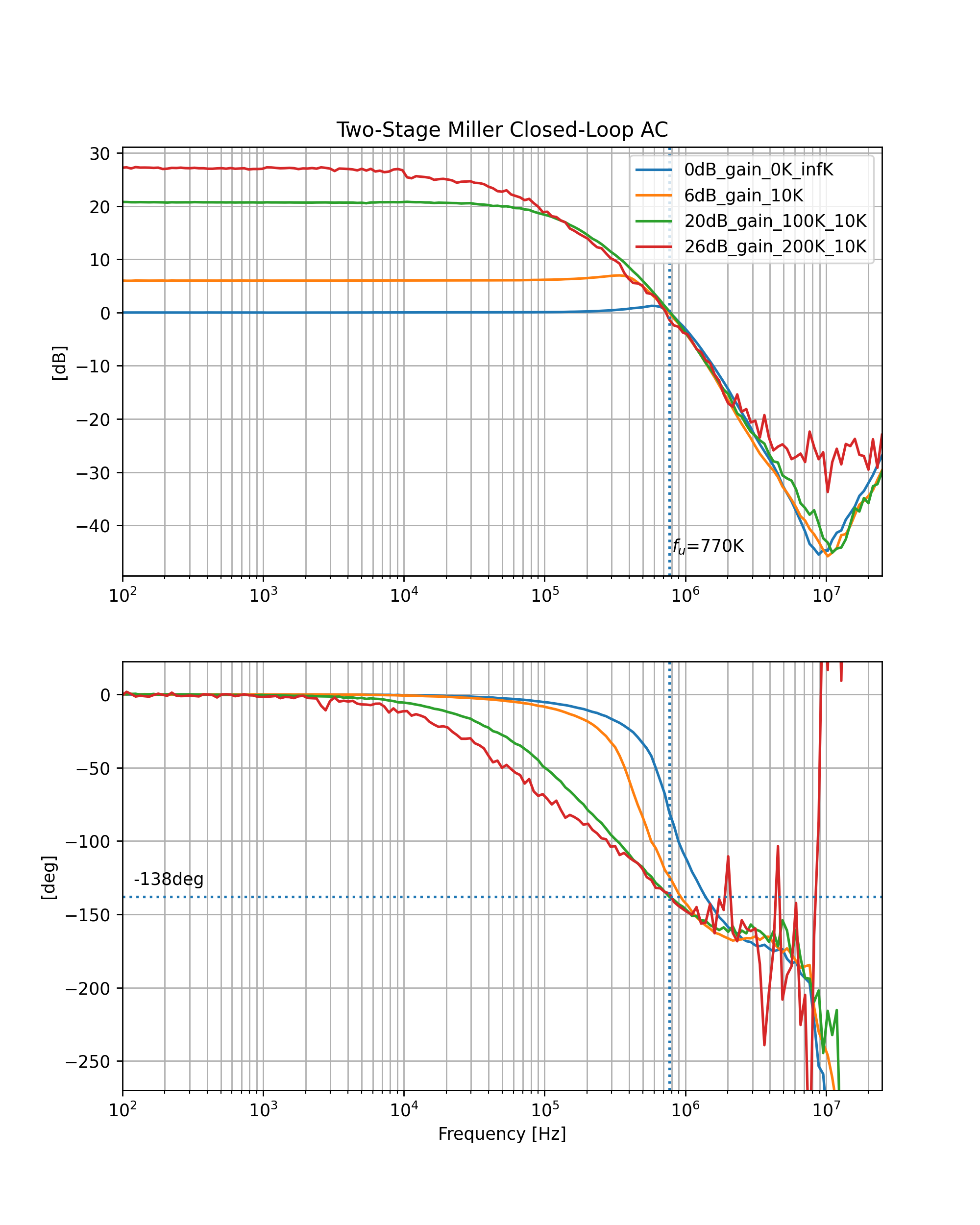
We measured the frequency response of the OTA in various feedback configurations. The feedback resistor from the OTA output to the negative input is varied to 200K, 100K, 10K, and short (OK), while the resistor from OTA negative input to AC ground (1uF cap) is kept at 10K and removed for the unity-gain configuration (0K); we expect gains of 21x, 11x, 2x, 1x or 26.4, 20.8, 6 and 0dB. With the negative input connected through a resistor and capacitor to ground, the OTA is always in unity gain for DC which avoids amplification of the offset.
The ADALM2000 network analyzer function is used with the generator W1 connected to the positive input of the OTA. The amplitude is adjusted to avoid out-of-range signals on the outputs; lower amplitudes are used for the higher gain cases; as a result, the high frequency measurement accuracy degrades in those cases.
The measurements were saved in .csv files an plotted with a python Jupyter notebook. Beyond their respective bandwidth we expect the transfer functions to overlap, and this can indeed be observed in the magnitude and phase response. As expected the various transfer functions have a similar unity-gain frequency \(f_u\) of about 770KHz. Beyond the bandwidth we measure close to the open-loop transfer function. At 770KHz the phase shift on the 26dB transfer function is -138deg, which can be used to estimate a phase margin for the 0dB case of approx. 42deg. The magnitude of the 0dB transfer function indeed shows some peaking.
Step Responses#
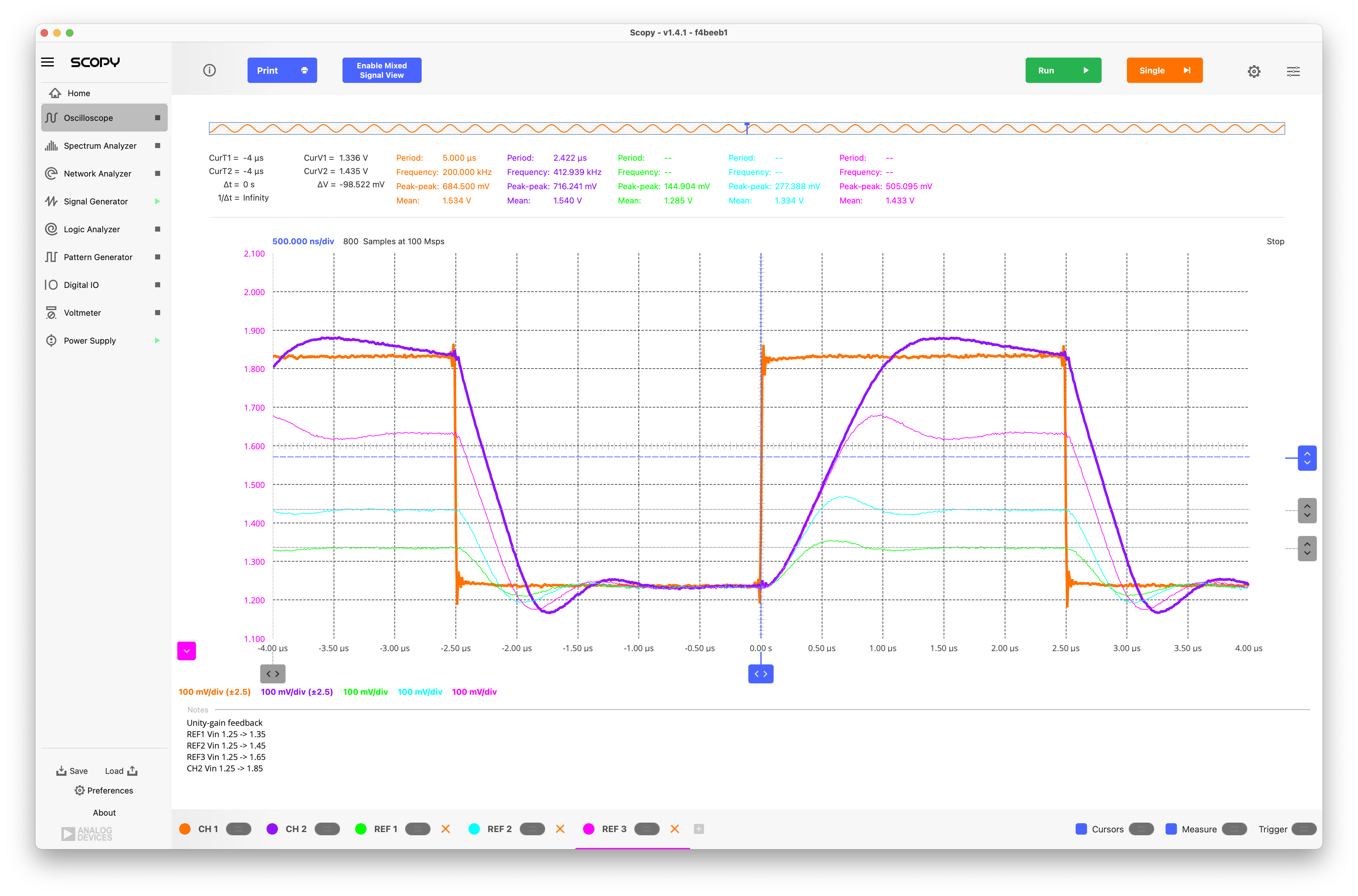
Fig. 2.21 At t=0s, positive step responses of the OTA configured as a unity-gain buffer. Notes provided a legend for the traces#
Positive step responses are collected for the unity-gain case with the OTA output connected to the negative input; the signal generator W1 is connected to the positive OTA input and and generates 200KHz square waves between 1.25V and 100mV, 200mV, 400mV and 600mV higher.
As expected for the given phase margin, we do see some overshoot. The 100mV to 200mV step response scales linearly, however the higher amplitude step responses show the presence of slewing.
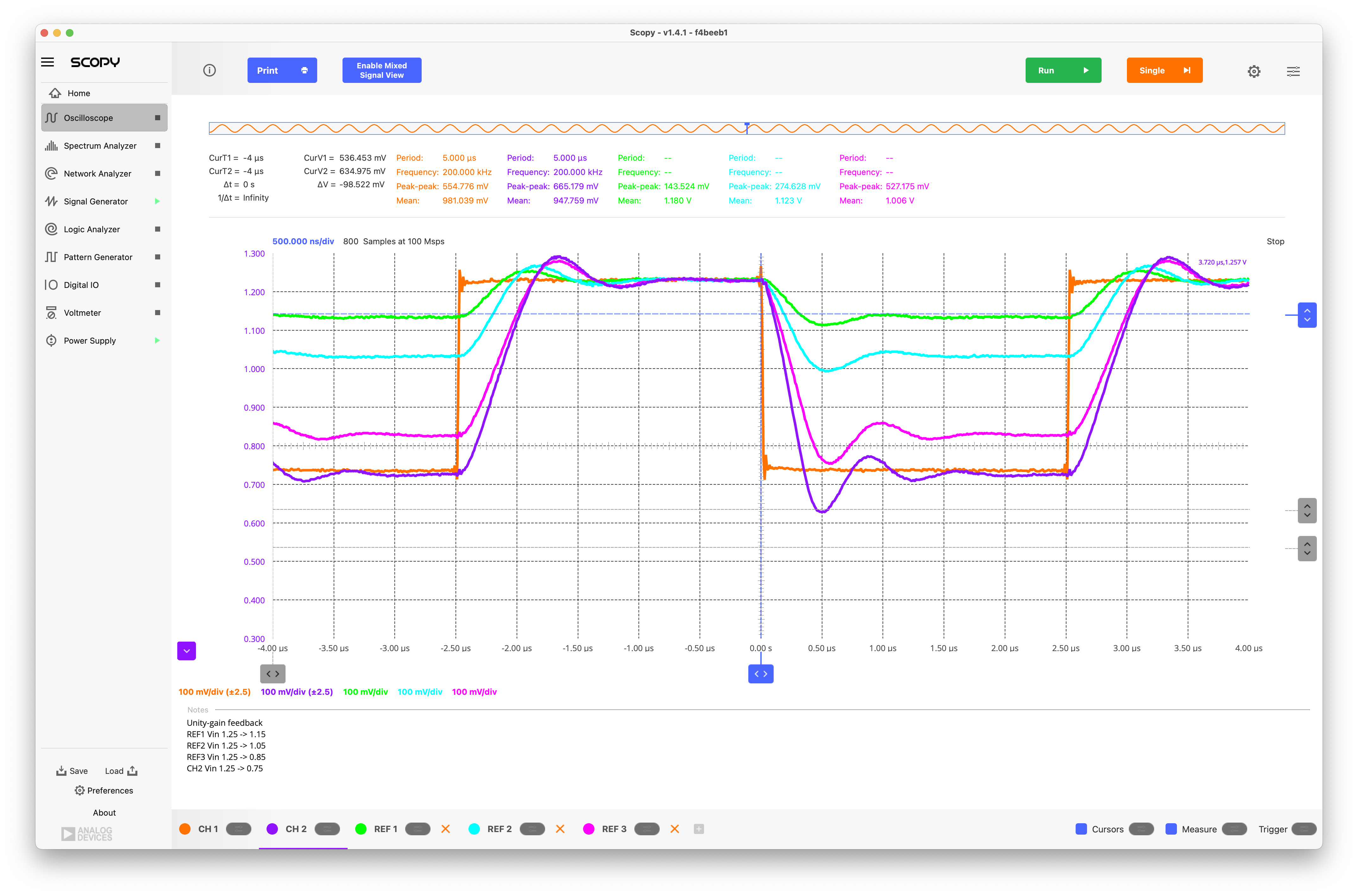
Fig. 2.22 At t=0s, negative step responses of the OTA configured as a unity-gain buffer. Notes provided a legend for the traces#
For the negative step responses, the signal generator W1 generates 200KHz square waves between 1.25V and 100mV, 200mV, 400mV and 500mV lower.
As expected for the given phase margin, we again see some overshoot. The 100mV to 200mV step response scales linearly, however the higher amplitude step responses show the presence of slewing, although less than for positive steps.
Non-Inverting Configuration with 11x Gain#
We configure the OTA as a non-inverting 11x amplifier by connecting a 100K resistor between the output (BUS04) and the gate of M1 and a 10K resistor between the gate of M1 and a 1.25V DC bias; the bias is generated with a 20K potentiometer between VDD and VSS and a 47uF decoupling cap to VSS.
DC Transfer Characteristic#
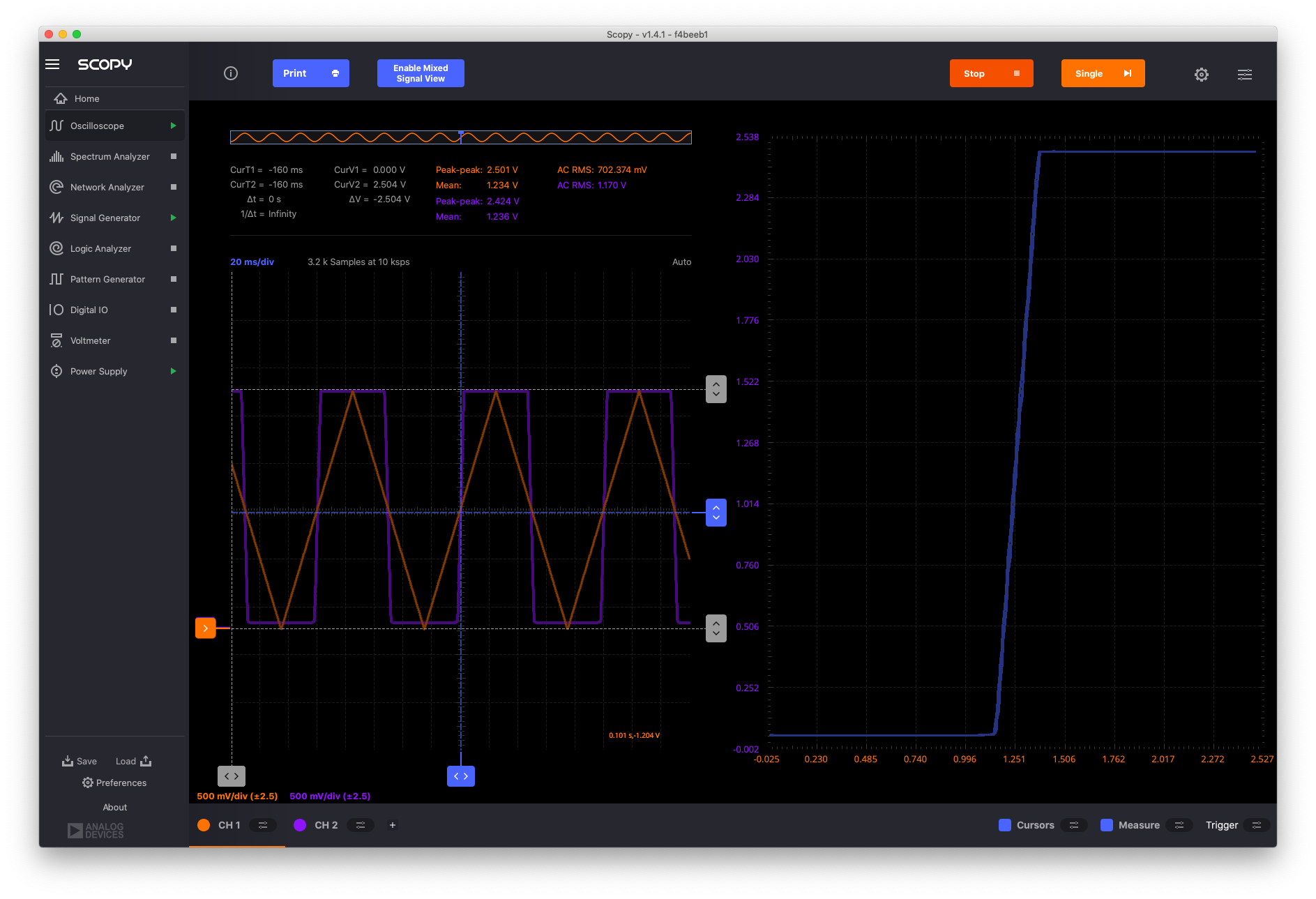
Fig. 2.23 DC transfer characteristic measured with a low-frequency rail-to-rail sawtooth input#
<TBD Need to add the signal range measurements of the internal nodes>
Frequency Response#
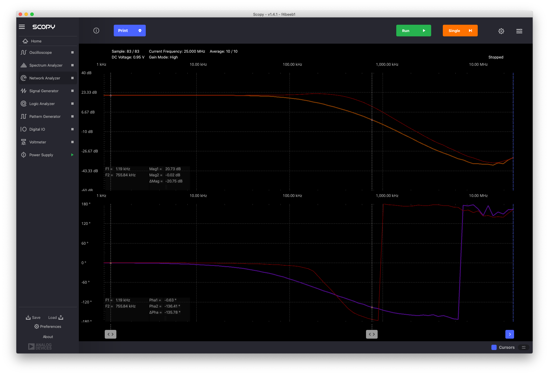
Fig. 2.24 Measured AC transfer characteristic of the compensated amplifier (purple) and uncompensated amplifier (red) in a 10x non-inverting configuration#
The DC gain is 20.7dB (10.8x), the unity-gain frequency, \(f_u\), is 756kHz, and the phase shift at \(f_u\) is -(180-44)deg. Note that we are doing a closed-loop measurement but above the 3dB bandwidth of the amplifier (i.e. the unity-gain frequency of the loop gain), the closed-loop response is close to the open-loop response.
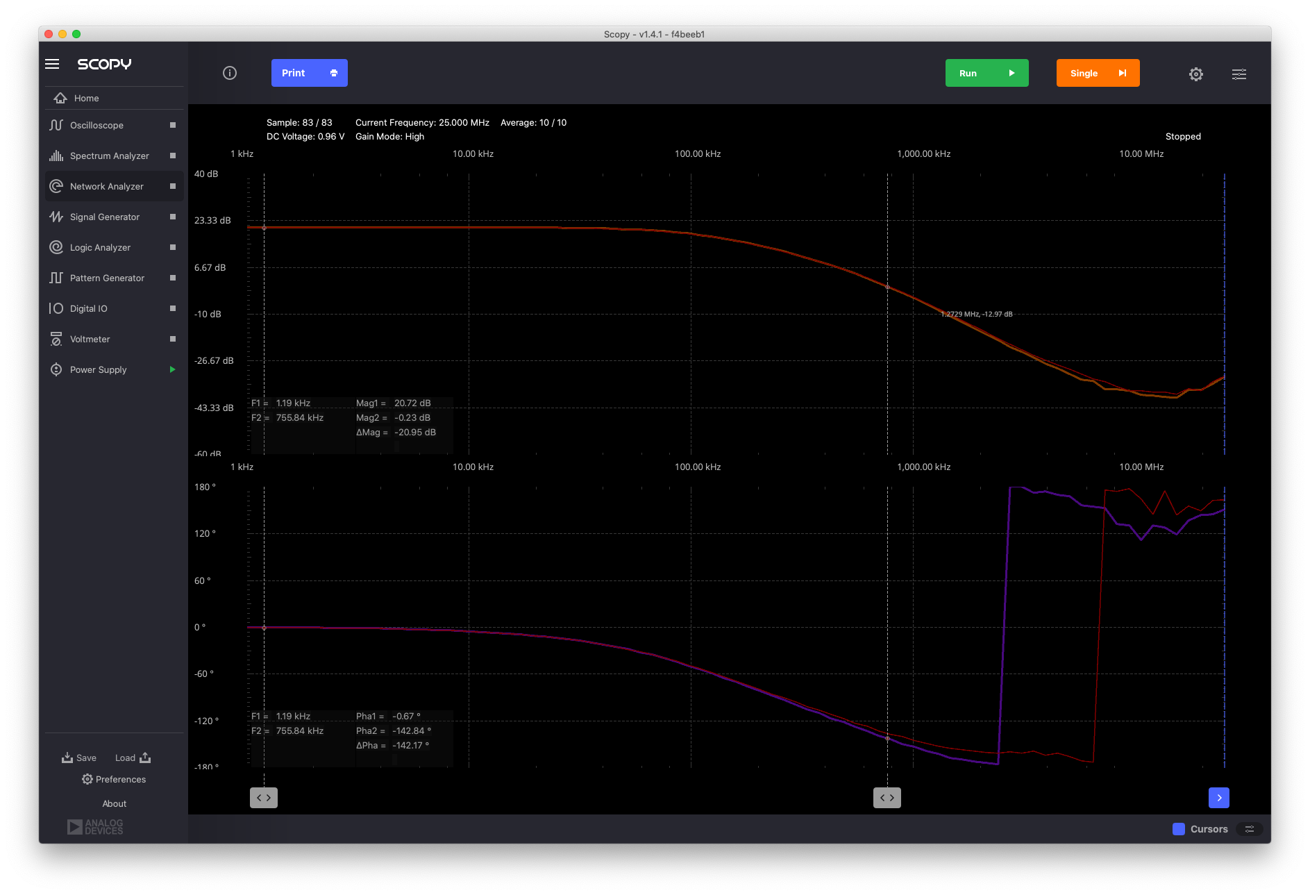
Fig. 2.25 Measured AC transfer characteristic of the compensated amplifier without \(R_{comp}\) (purple) and compensated amplifier (red) with \(R_{comp}\) in a 10x non-inverting configuration#
Step Response#
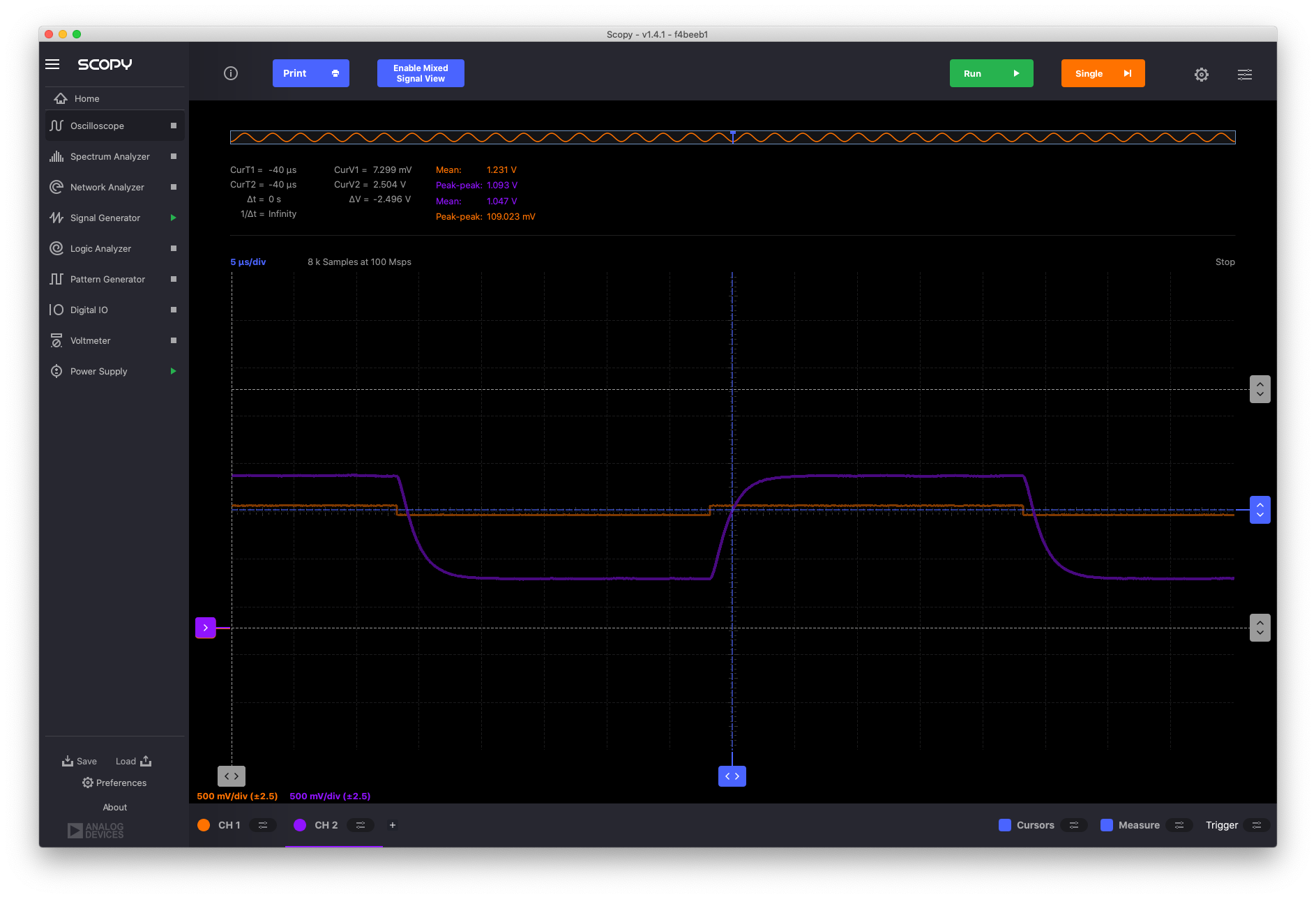
Fig. 2.26 Measured step response of the compensated amplifier (purple) in a 10x non-inverting configuration for a 100mVpp input signal#
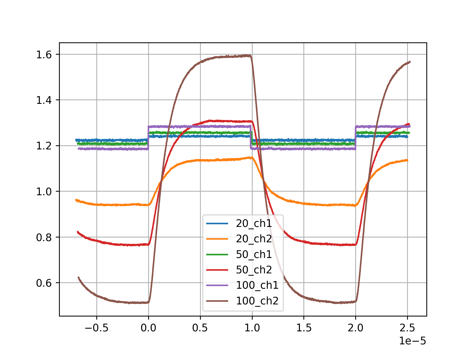
Fig. 2.27 Measured step responses of the compensated amplifier in a 10x non-inverting configuration for a 20, 50 and 100mVpp input signal around 1.25V common mode[2]#

Fig. 2.28 Measured step response of the uncompensated amplifier (purple) in a 10x non-inverting configuration for a 100mVpp input signal#
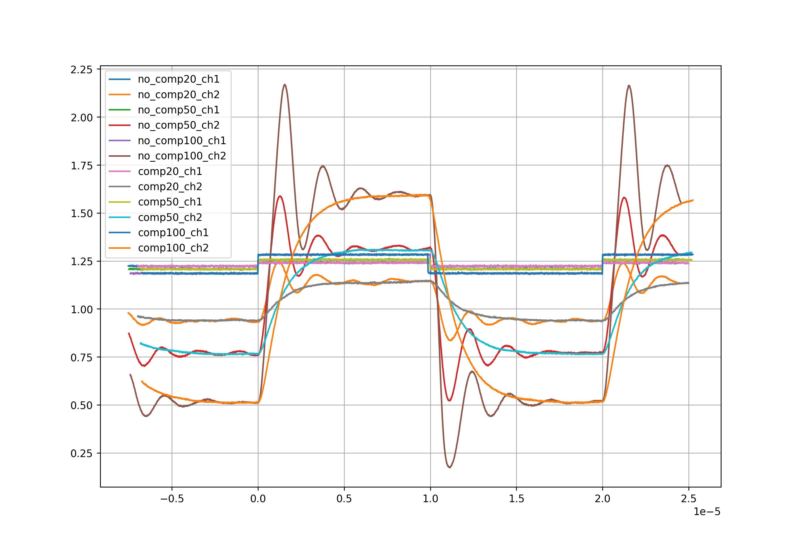
Fig. 2.29 Measured step responses of the compensated and uncompensated amplifier in a 10x non-inverting configuration for a 20, 50 and 100mVpp input signal around a 1.25V common mode#
Measuring Offset and DC Gain#
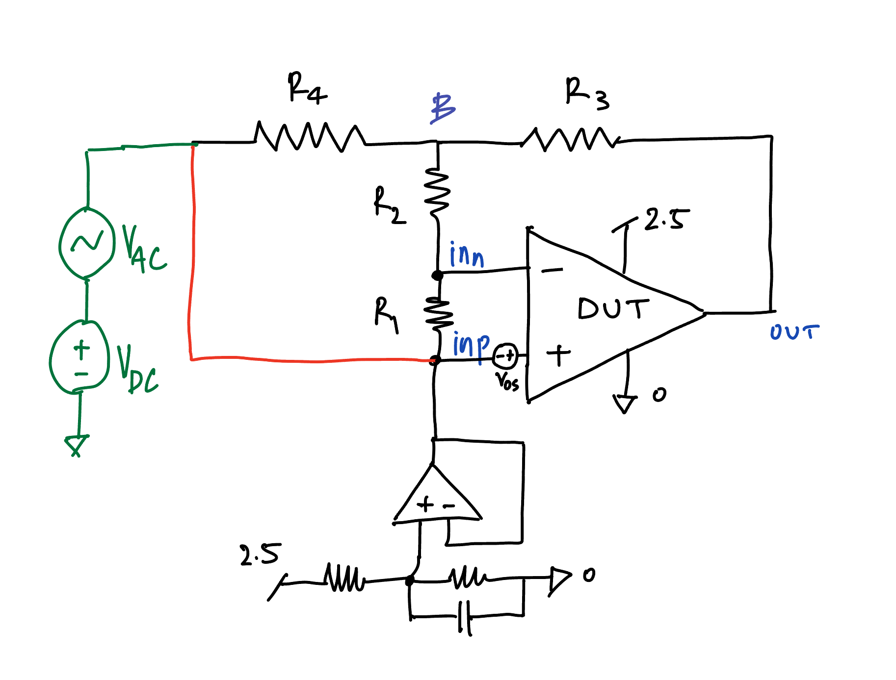
Fig. 2.30 A circuit setup to measure the offset (keep red, remove green) and DC gain (keep green, remove red) of an operational amplifier; we used R1=1K, R2=100K, R3 = R4 = 10K#
Offset Measurement#
Assuming R4 \(\ll\) R2, the offset voltage \(V_{os}\) will appear between ‘B’ and ‘inp’ as \((1+R2/R1)V_{os}\) or \(101 V_{os}\) and between ‘out’ and ‘inp’ as \(2(1+R2/R1)V_{os}\) or \(202 V_{os}\) with R1 = 1K, R2 = 100K, and R3 = R4 = 10K. An AD8542 was configured in unity-gain feedback to buffer the common-mode voltage of 1.25V and apply it to ‘inp’.
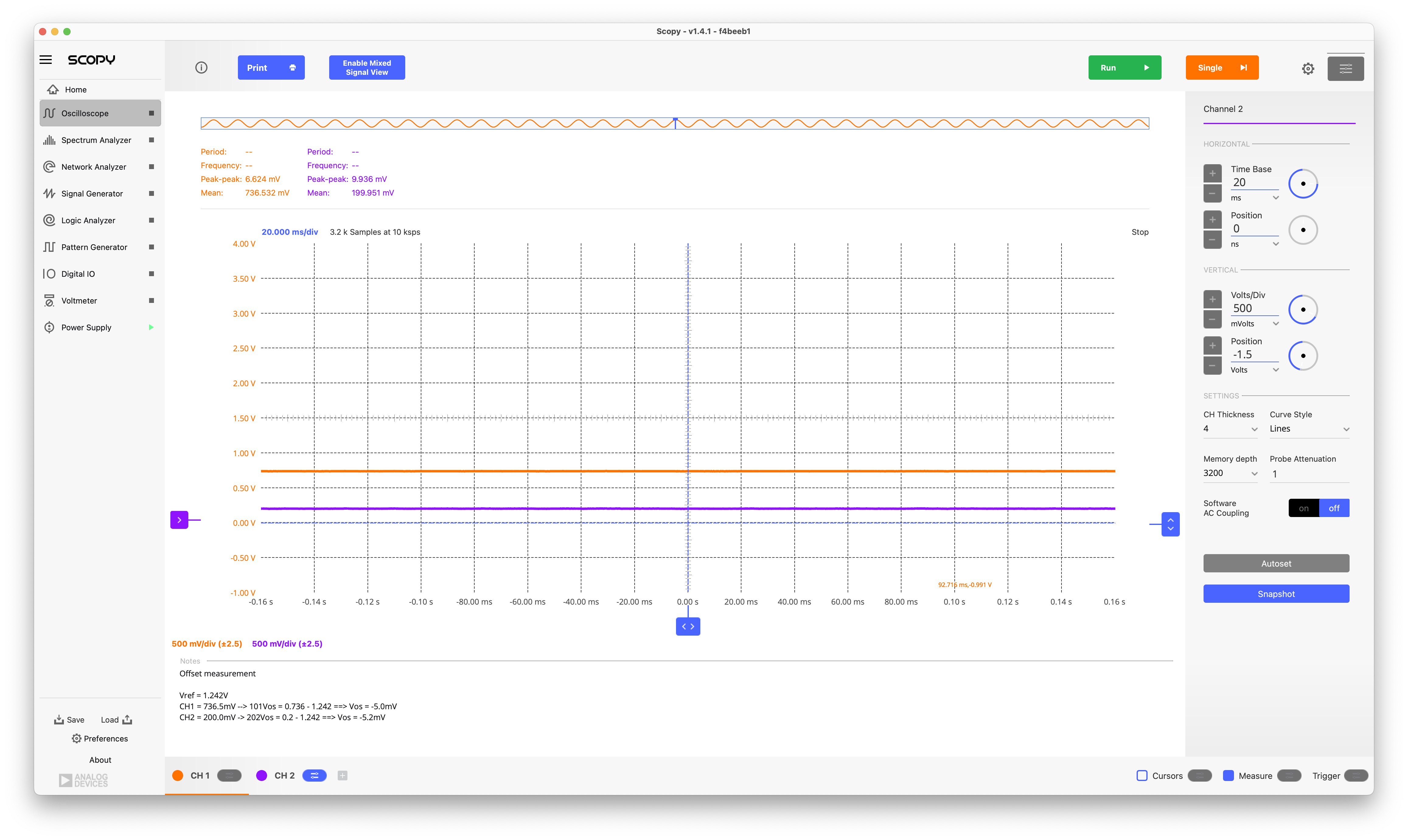
Fig. 2.31 Oscilloscope traces obtained for the DC offset measurement#
The measured voltages at ‘B’ (CH1) and ‘out’ (CH2) compared to ‘inp’ result in an offset measurement of -5.0mV and -5.2mV respectively. We note that the resistors used were 5% resistors.
This offset is a combination of the systematic and random offset. Mulitple chip samples need to be measured to separate the systematic and random offsets.
DC Gain Measurement#
We apply a VDC of approximately 0.5V and an 100Hz sinusoid of 200mVpp and then measure the voltage at ‘B’ and ‘out’; VDC is adjusted to make sure the ‘out’ is within the output range of the amplifier.
Assuming R4 \(\ll\) R2, \(( V_{out} - V_{inp} ) = -R3/R4 (V_{AC} - V_{inp})\) so the AC gain is about \(-2\). The voltage between ‘inp’ and ‘inn’ is \(V_{out}/A\), so the voltage between ‘B’ and ‘inp’ is \(-(1+R2/R1)V_{out}/A\) or \(-101 V_{out}/A\).
The ratio \(V_{out, AC} / V_{B, AC} = -A/101\)
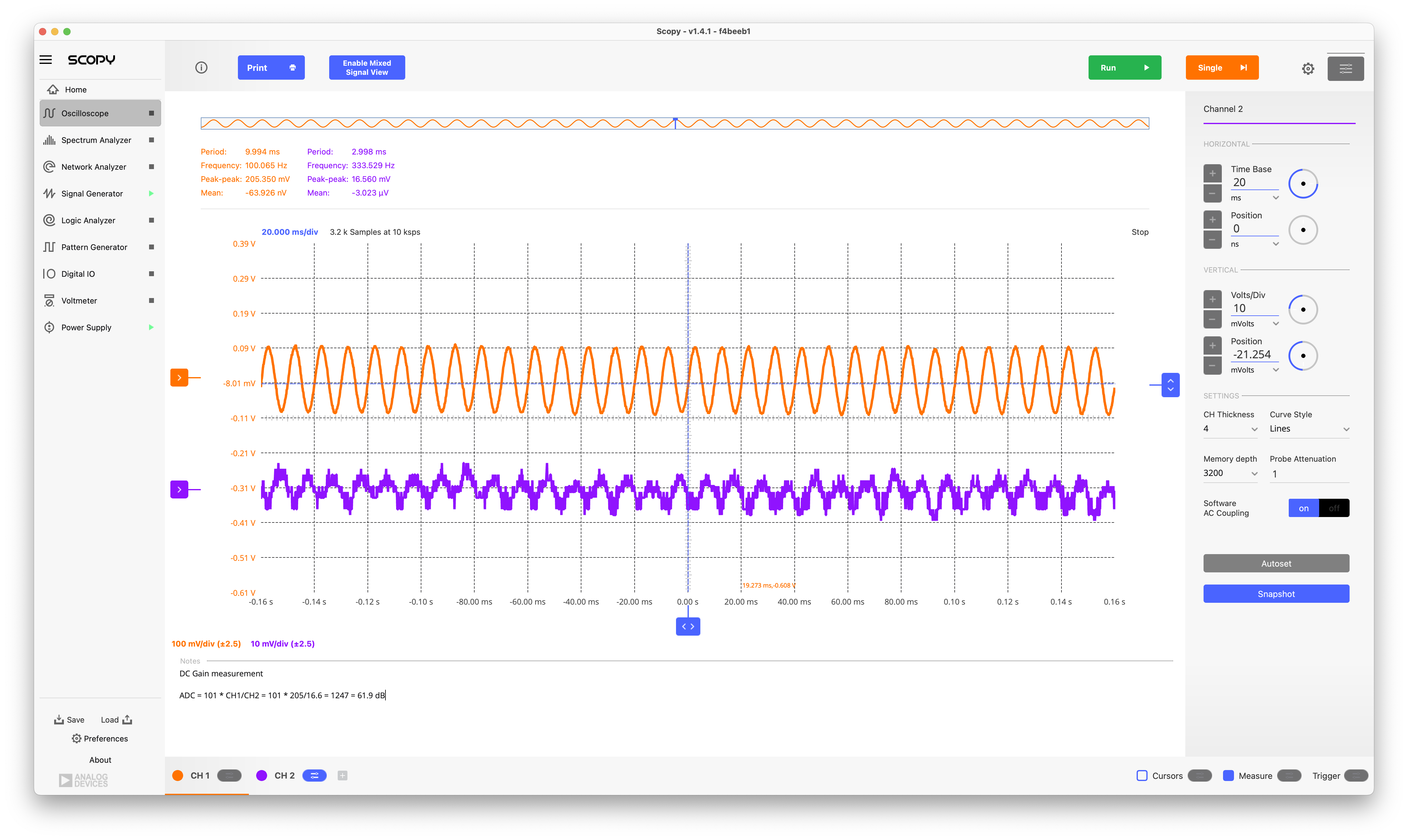
Fig. 2.32 Measurement of ‘out’ (CH1) and ‘B’ (CH2) on the oscilloscope with a 100Hz input signal; the channels are AC coupled#
Estimating the amplitude of the waveform at ‘B’ is difficult in the time domain using the oscilloscope.
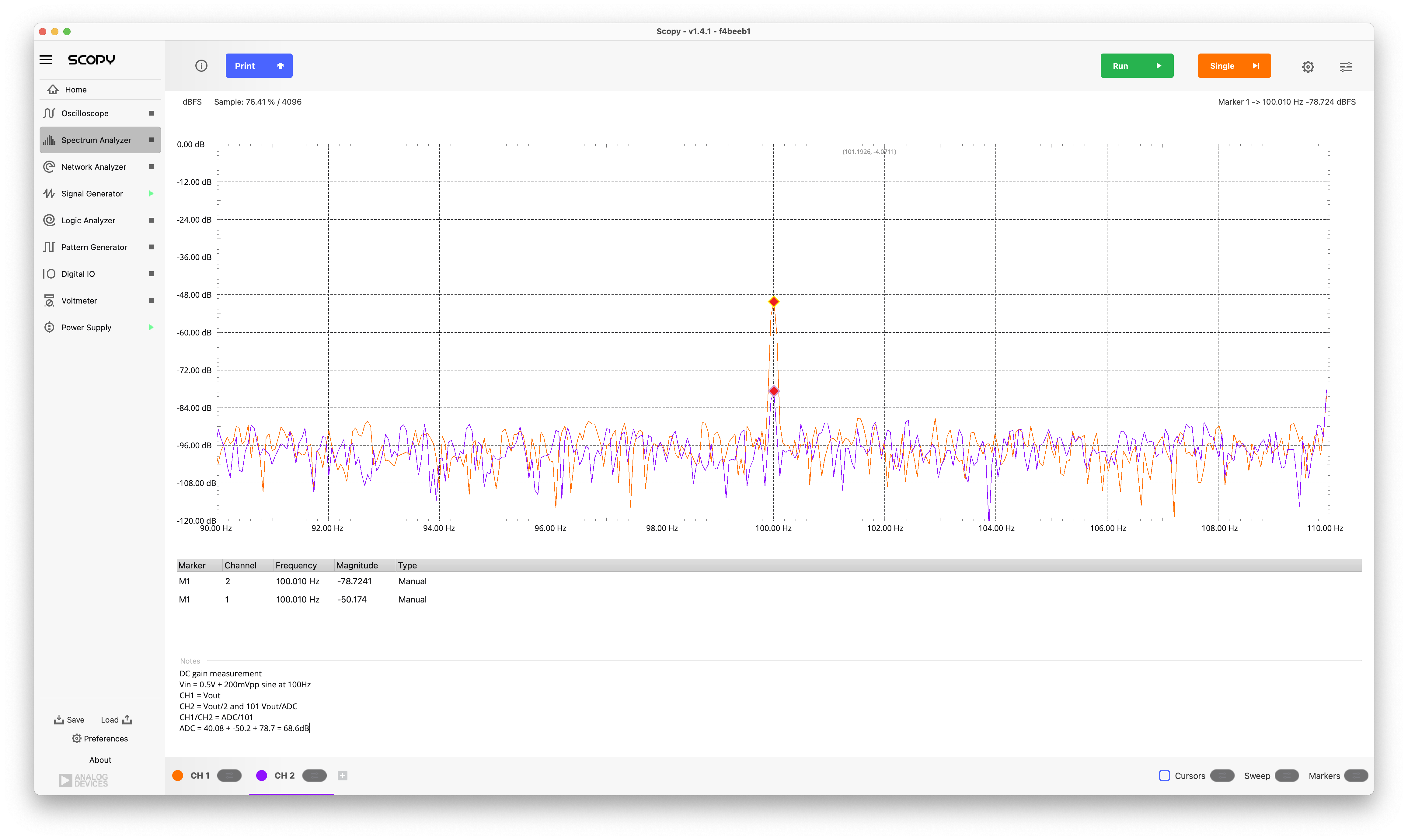
Fig. 2.33 Measurement of ‘out’ (CH1) and ‘B’ (CH2) on the spectrum analyzer with a 100Hz input signal#
Using the spectrum analyzer, a better estimate of the ratio of \(V_{out, AC} / V_{B, AC} \) can be obtained, and the OTA gain \(A\) at 100Hz is estimated to be 68.6dB.
Studying the Frequency Response#
Measuring the Open-Loop Transfer Function#
Measuring the open-loop transfer function of the OTA requires a careful setup in to address the issues of DC offset and the very large gain to be measured, possibly requiring very small reference signal sources.
The OTA is configured with an \(C_L\) of 1nF, a \(C_{comp}\) of 150pF, and an \(R_{comp}\) of 200\(\Omega\). We embed the OTA in the following test schematic that addresses the measurement challenges:
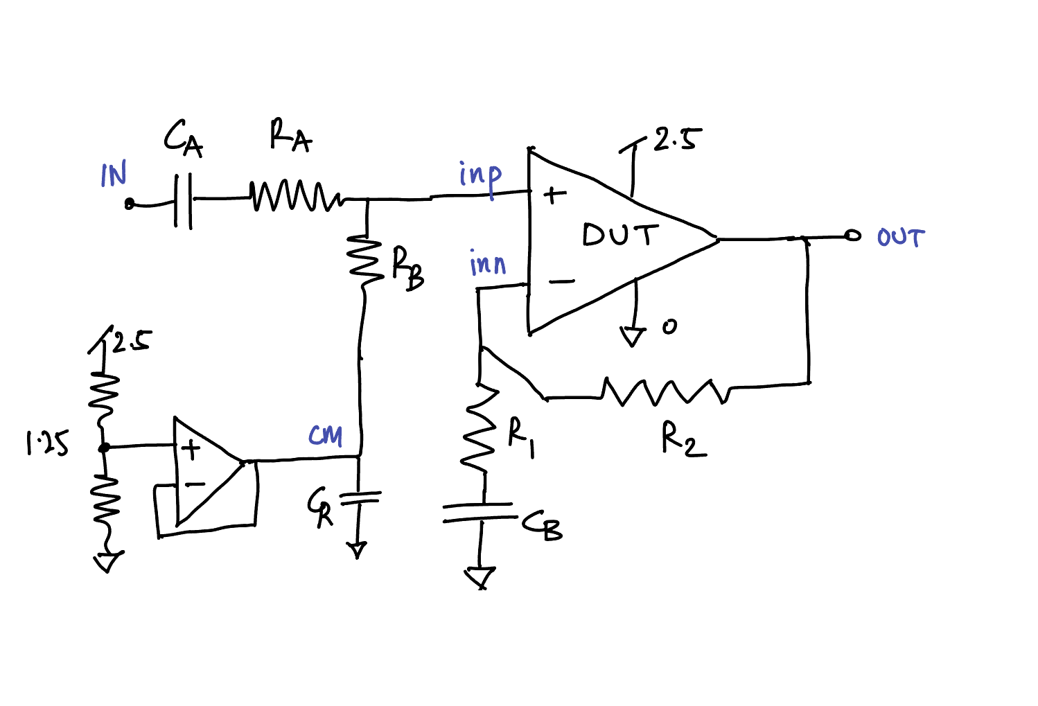
Fig. 2.34 Test setup to measure the AC loop gain of the OTA; RA = 100K, RB = 1K, CA = 1uF; R2 = 1M and R1 is varied from 10K, 1K, to 100 to change the in-band gain; CB = 22uF//1uF; buffer amplifier is the AD8542 and CR = 1uF#
The resistive divider R1, R2 from the output ‘OUT’ to the negative input ‘inn’ sets the AC closed-loop gain to \((1+R2/R1)\). However, we do not connect R1 to the common-mode, mid-supply voltage ‘cm’, but rather to a large capacitor CB of (1uF // 22uF). As a result, for DC and at very, very low frequencies the OTA is in a unity-gain feedback configuration, which is needed to avoid large amplification of the DC offset.
The resistive divider RA, RB attenuates the input signal. This allows for a larger AC coupled signal from the signal source which will improve measurement accuracy[3]. As long as we can rely on the input attenuation to be constant across the frequency range of interest, we can add it back to the measured gain from the signal source to the amplifier output to obtain the amplifier gain. RB connects to a buffered and decoupled common-mode, mid-supply reference.
We configured the amplifier for closed loop AC gains of 101x, 1001x, 10,001x and performed network analysis measurements using the ADALM2000 between ‘IN’ and ‘OUT’, making sure to adjust the input signal amplitude to avoid out-of-range signals at the output.
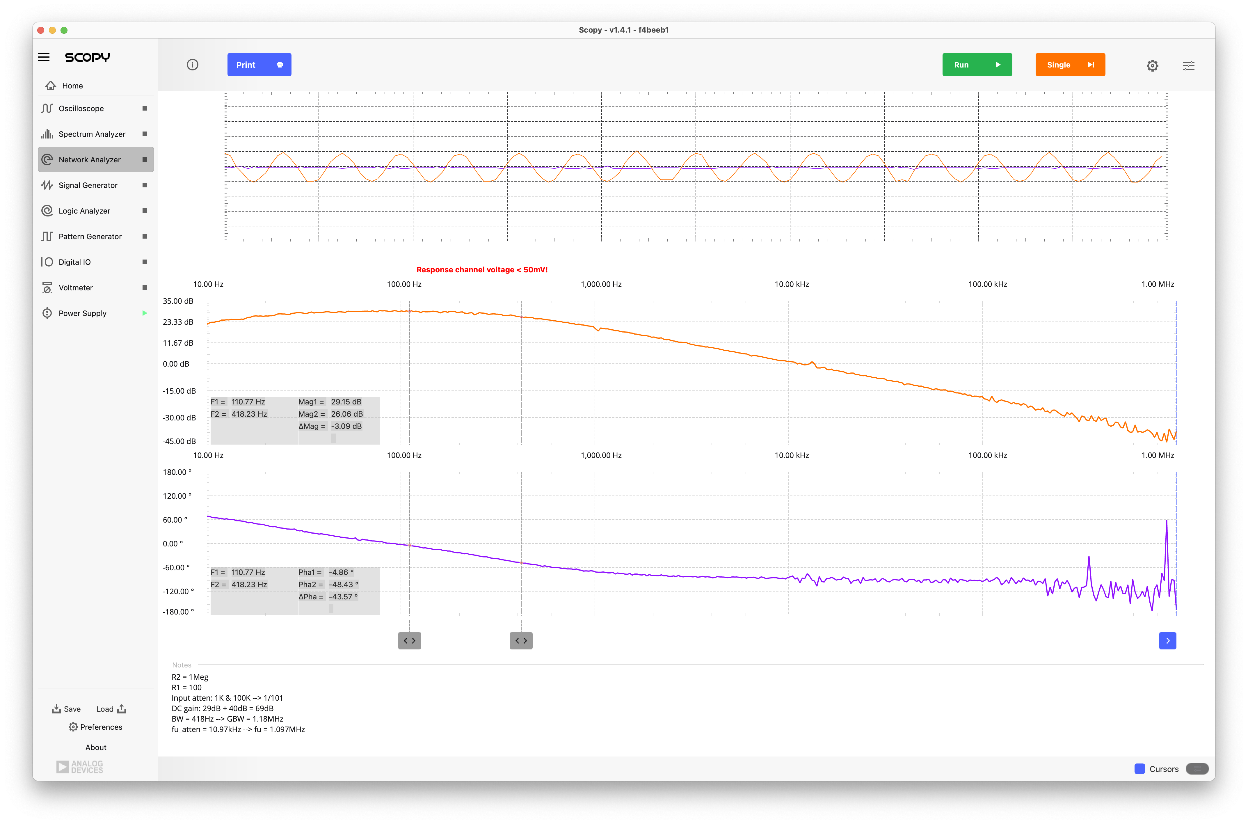
Fig. 2.35 Bode plot of the gain with the amplifier configured for a 10,001x gain (orange/purple); note that there is a 40dB attenuation of the input signal#
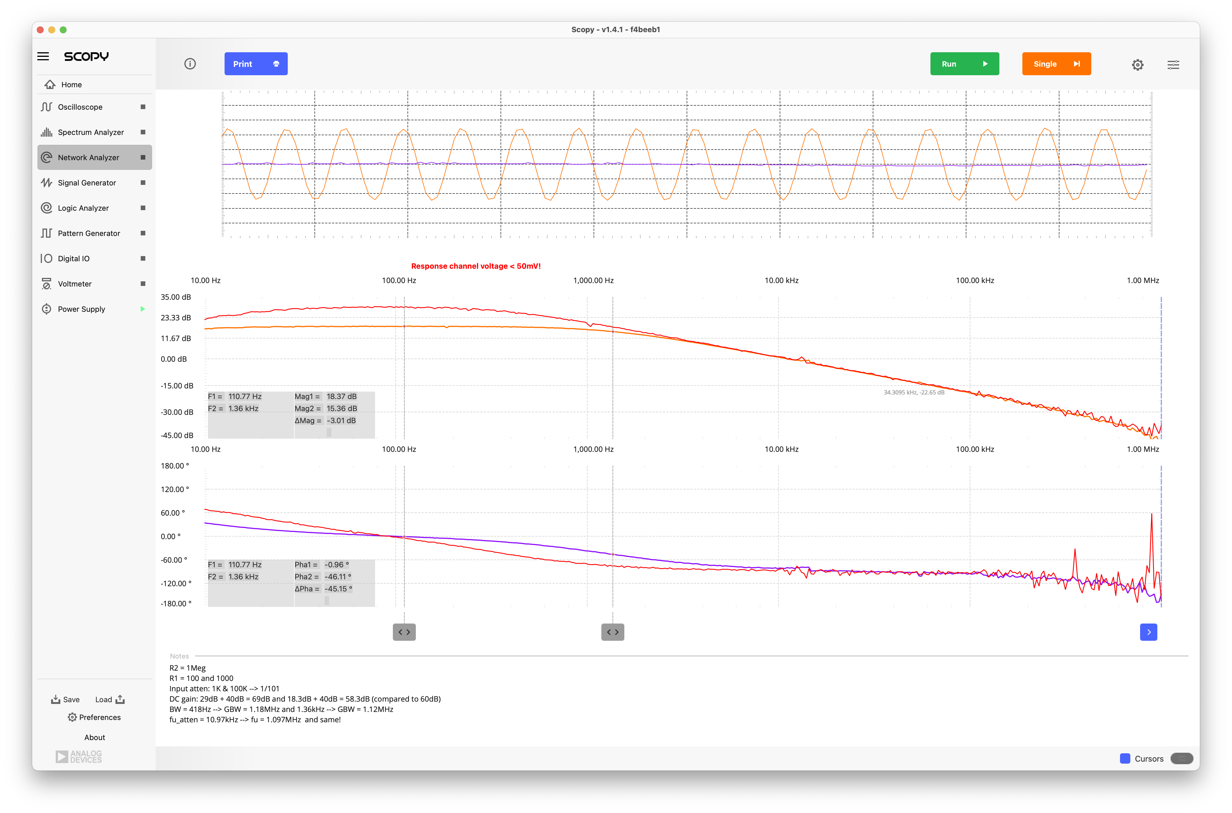
Fig. 2.36 Bode plot of the gain with the amplifier configured for a 1001x gain (orange/purple) compared to the 10,001x gain case; note that there is a 40dB attenuation of the input signal#
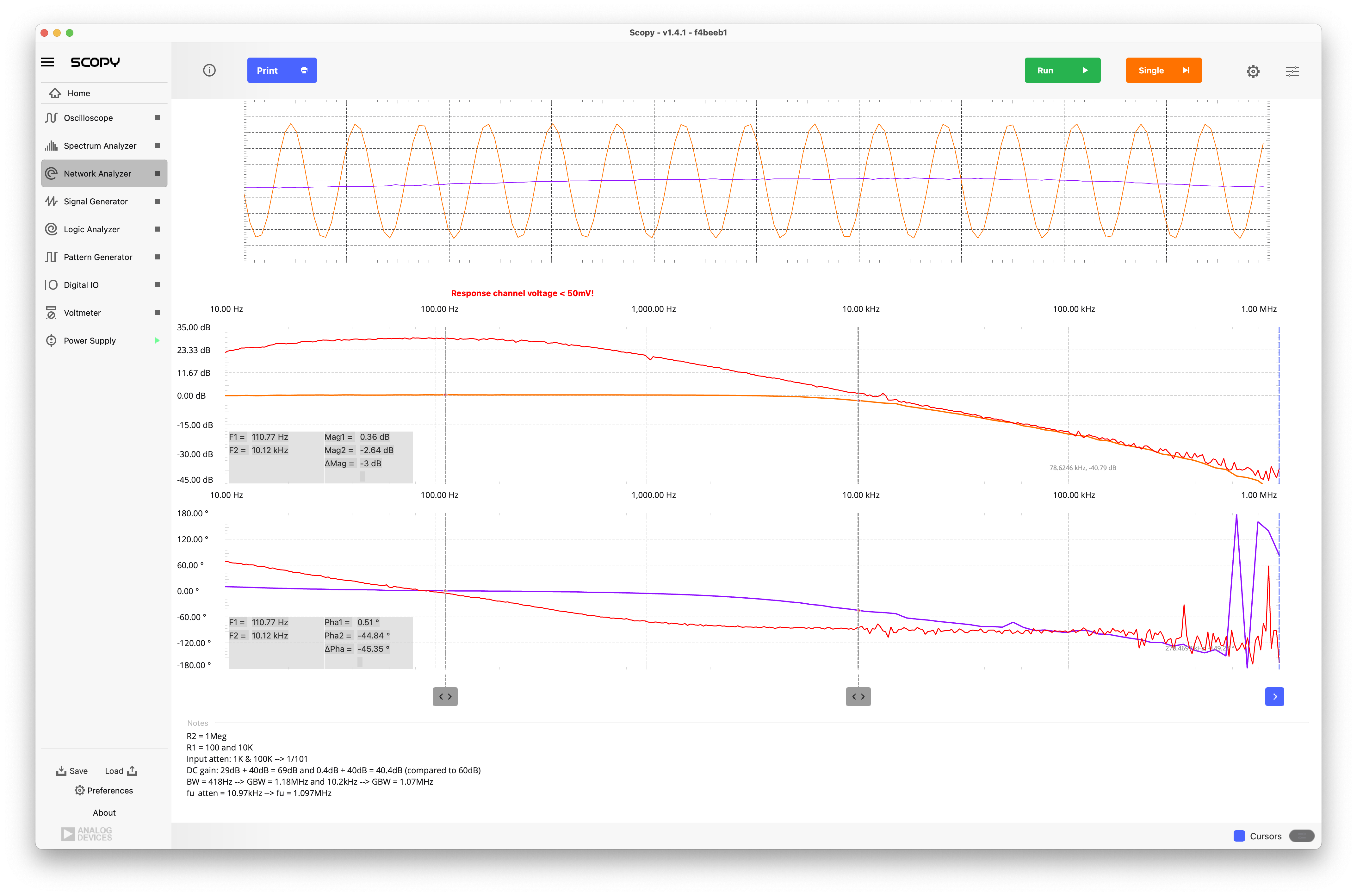
Fig. 2.37 Bode plot of the gain with the amplifier configured for a 101x gain (orange/purple) compared to the 10,001x gain case; note that there is a 40dB attenuation of the input signal#
DC Gain#
We note that for the 10,001x gain case, the low-frequency gain is limited by the DC gain of the OTA; at 100Hz we measure a DC gain of 69dB.
Unity-Gain Frequency#
All plots overlap at high frequencies and indicate a unity gain frequency of about 1.10MHz for the open-loop OTA; the notes under the plots analyze the various ways to measure the unity-gain frequency as the LF gain times the bandwidth vs the frequency at which the gain reaches -40dB; all cases give very similar results likely within the measurement accuracy of the setup.
The Effect of a Zero-Compensation Resistor#
<Preliminary, needs more description and work>
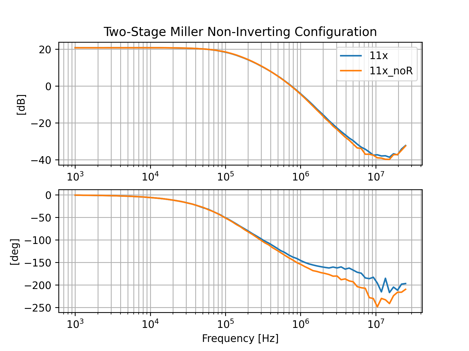
Fig. 2.38 The frequency response of the OTA configured as a 11x non-inverting amplifier with a Miller compensation with a 200\(\Omega\) or no zero-compensation resistor#
Here we measure the effect of the zero-compensation resistor; we note an improvement in the phase response when the resistor is present. When the frequency is sufficiently above the 3dB frequency of the closed loop gain, we observe the open-loop phase response. The resistor improves the phase shift measurably.
Measuring the Input-Stage Transconductance#
The DC transfer characteristic of the input differential pair (M1, M2) requires the measurement of its differential output current w.r.t. a differential input voltage. We repurpose the second stage, M5, as a transresistance stage[4], by placing a 1K\(\Omega\) resistor R1 from drain to gate.
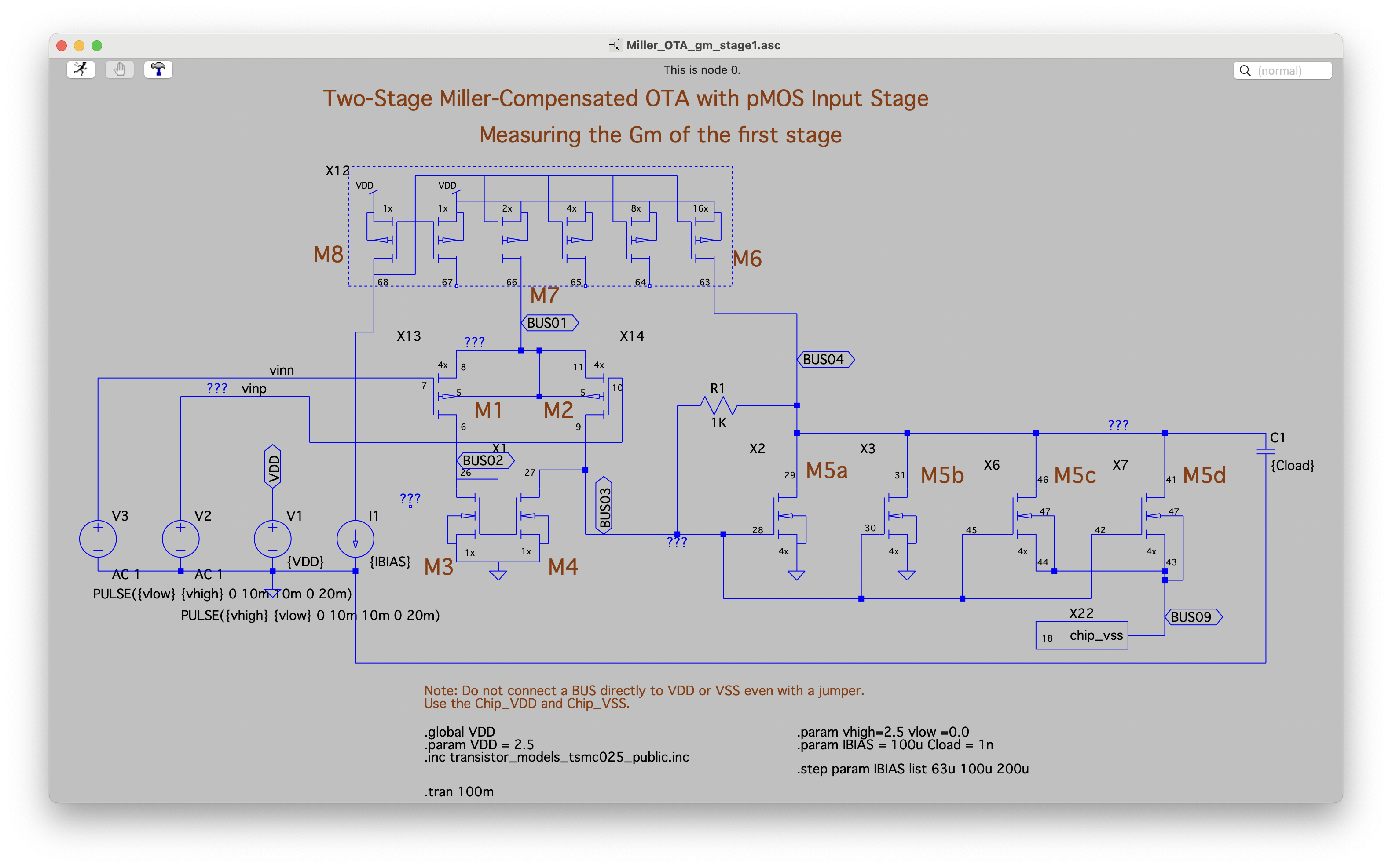
Fig. 2.39 The second stage, M5, is configured as a transresistance amplifier to measure the differential output current of the differential input pair (M1, M2) when driven with external input signals.#
We now apply a differential sawtooth waveform, with a common-mode of 1.25V, to the gates of M1 and M2 (using the waveform generators on the ADALM2000), and measure the gate and drain voltage of M5.
The gate voltage of M5 is not changing much, as expected since M5 acts as a transresistance stage. Any current pushed into the gate of M5 by M2 or M4 is going into the feedback resistor R1.
Measuring the voltage across the feedback resistor R1, we can determine the output current of the differential pair (M1, M2); the current mirror (M3, M4) takes the output of M1 and subtracts it from M2, the difference flowing into R1. With an X-Y plot on the oscilloscope we recognize the typical S-curve response of a differential pair.
We varied the bias current for the current-mirror diode M8 from 63uA to 100uA to 200uA. We saved the measurement results in .csv files which we imported into a python notebook and plotted the measured curves along with simulated curves. The correspondence is quite good, taking into account the limitations of the measurements, as well as the transistor models used for the simulation. We note that since this is a current-biased circuit, it is more robust.
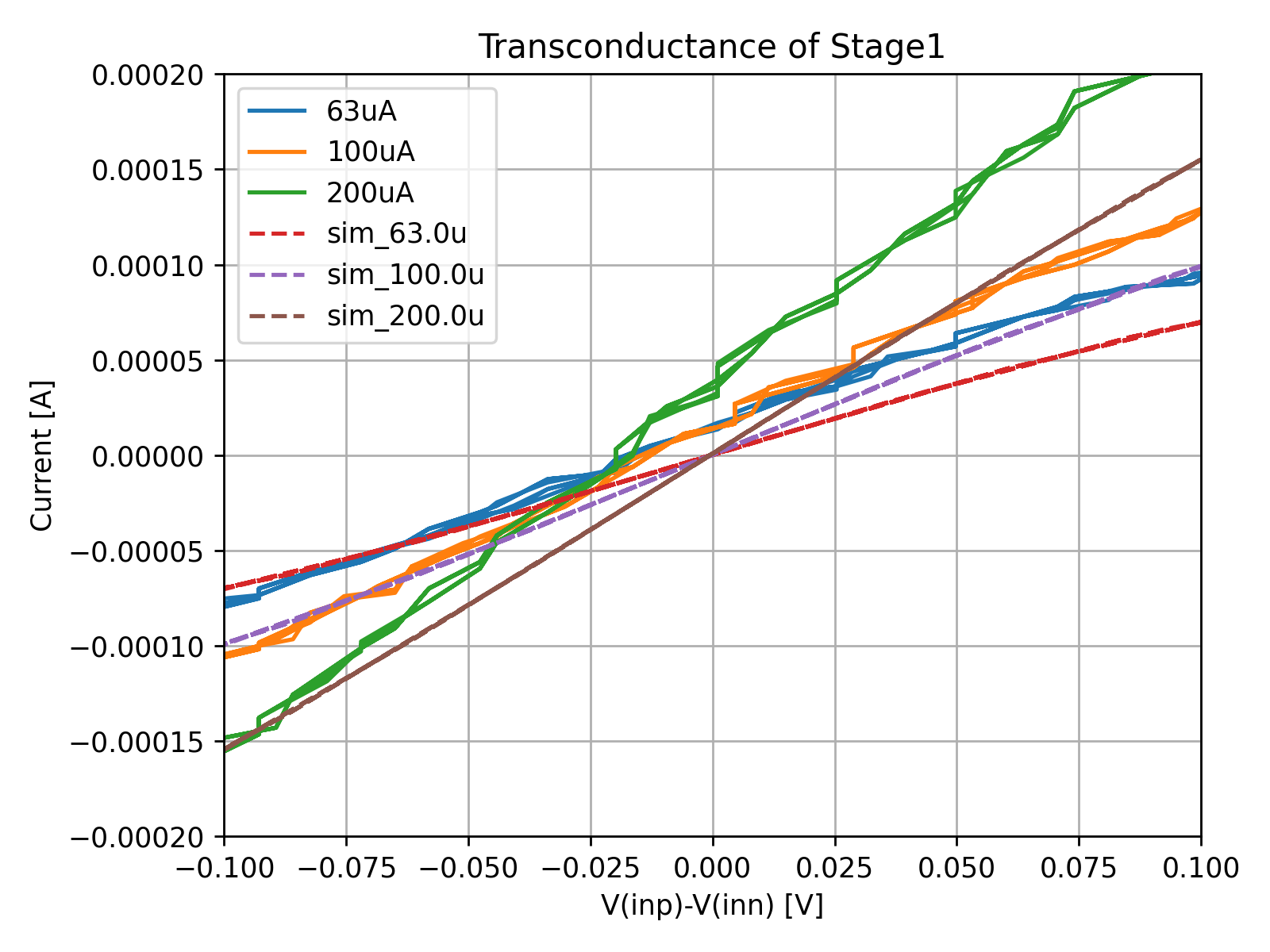
Zooming in around the origin we observe an offset of the differential pair of -10 to -15mV. There are better techniques to measure the offset, but this gives a rough estimate.
Additional Experiment Ideas#
This experiment can now be expanded to measure responses to common-mode input signals, or to measure responses across frequency.
A more sophisticated transresistance amplifier can be constructed to try to improve measurement accuracy. Averaging the waveforms will improve measurement accuracy as well.
Open-Loop Measurement with Low-Frequency OTA Feedback#
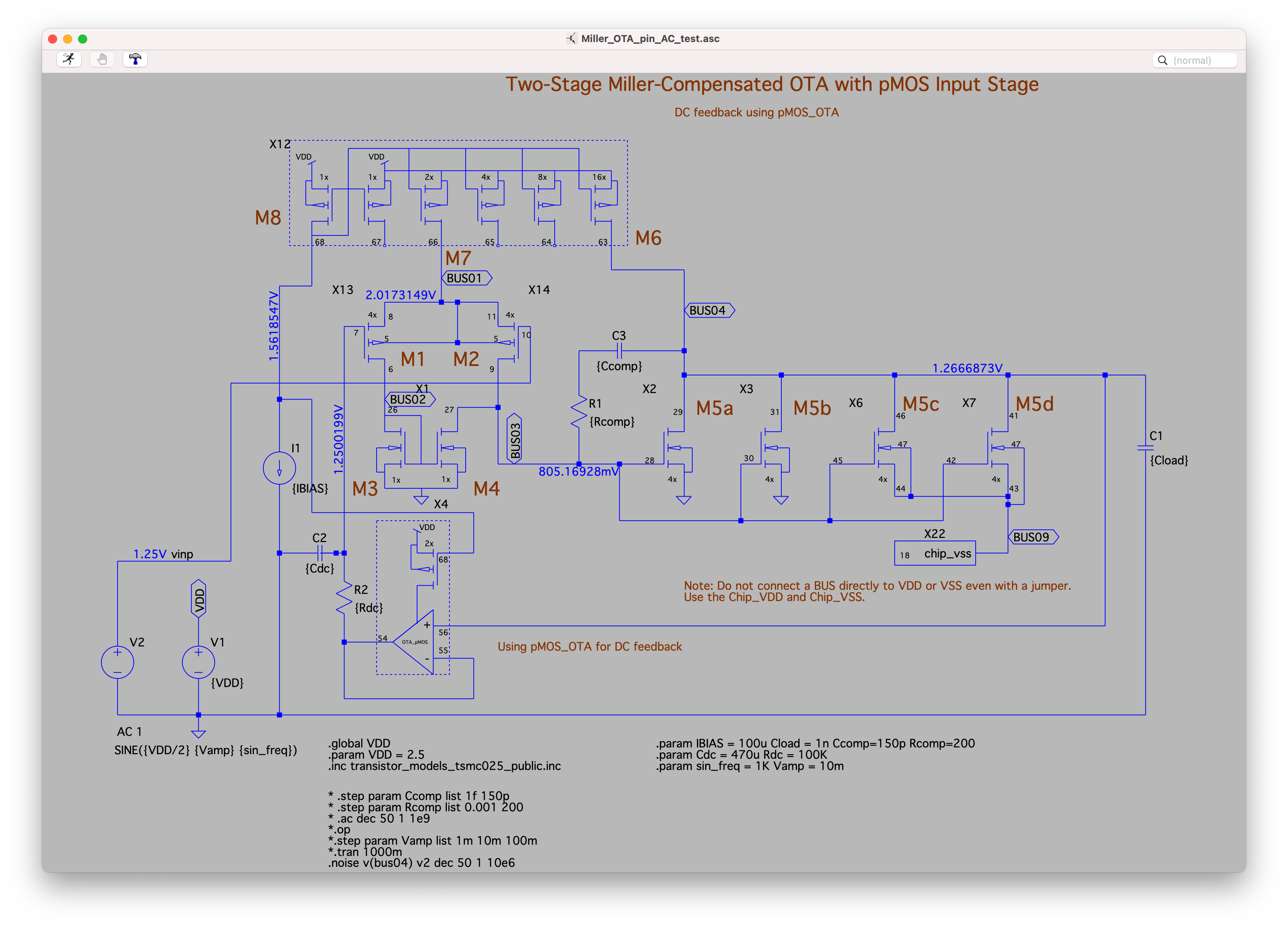
Fig. 2.40 The OTA is placed in DC feedback by using an active unity-gain buffer with a very low bandwidth#
When using a very low bandwidth active unity-gain feedback path, the OTA is in open loop for frequencies higher than \(A_{DC}/(2\pi R_{DC}C_{DC})\), where \(A_{DC}\) is the DC gain the OTA under test.
When applying no input signal, the OTA will amplify its own noise by its open-loop gain.
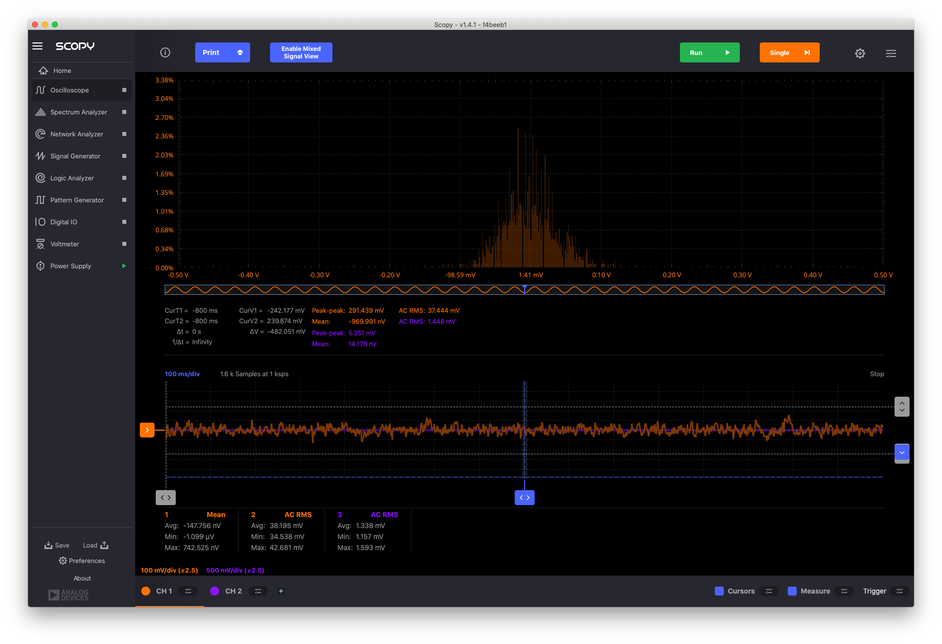
Fig. 2.41 The output of the OTA when placed in DC feedback but AC open loop; we observe the output noise of the OTA#
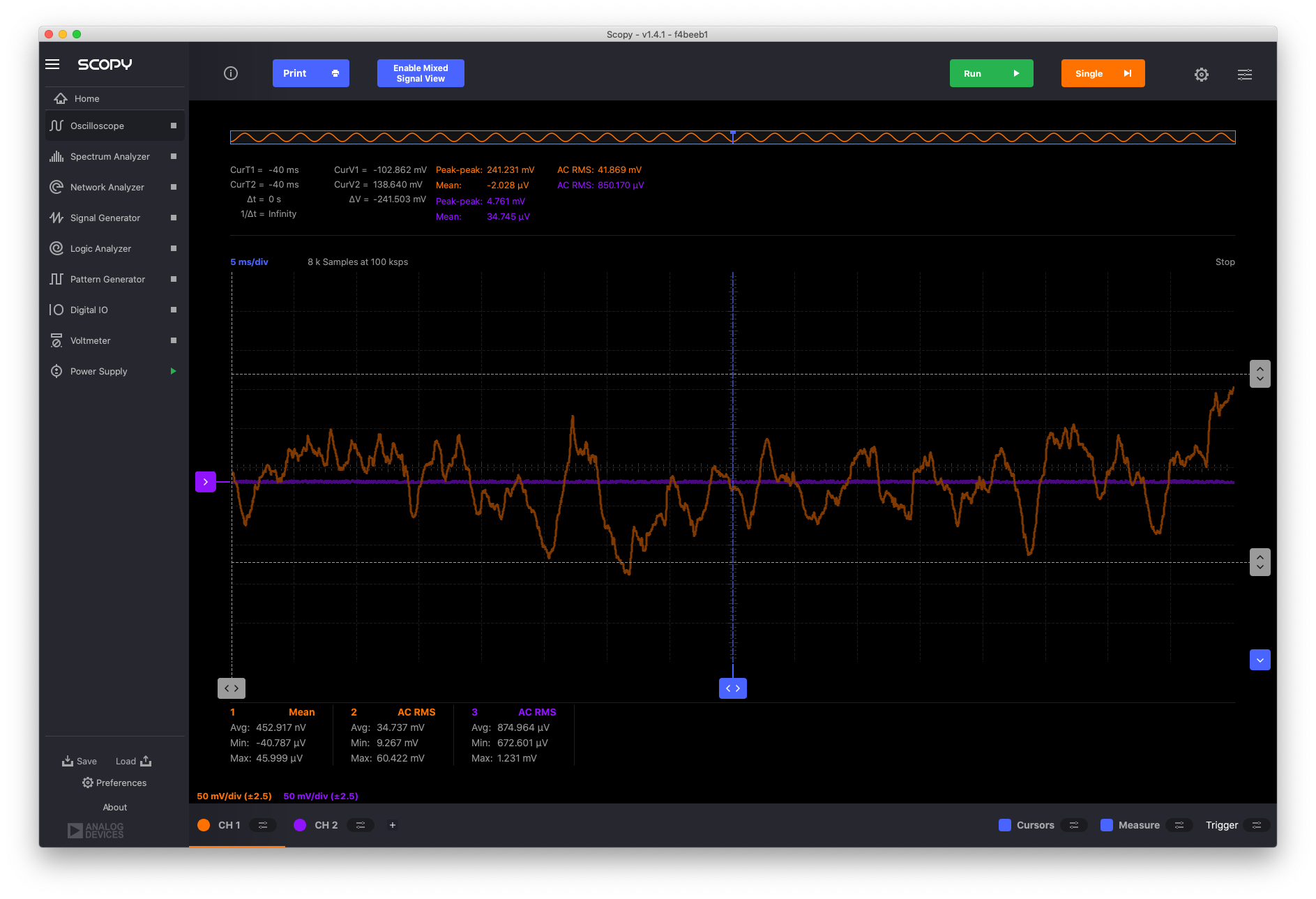
Fig. 2.42 The output of the OTA when placed in DC feedback but AC open loop; we observe the output noise of the OTA at a different time scale#
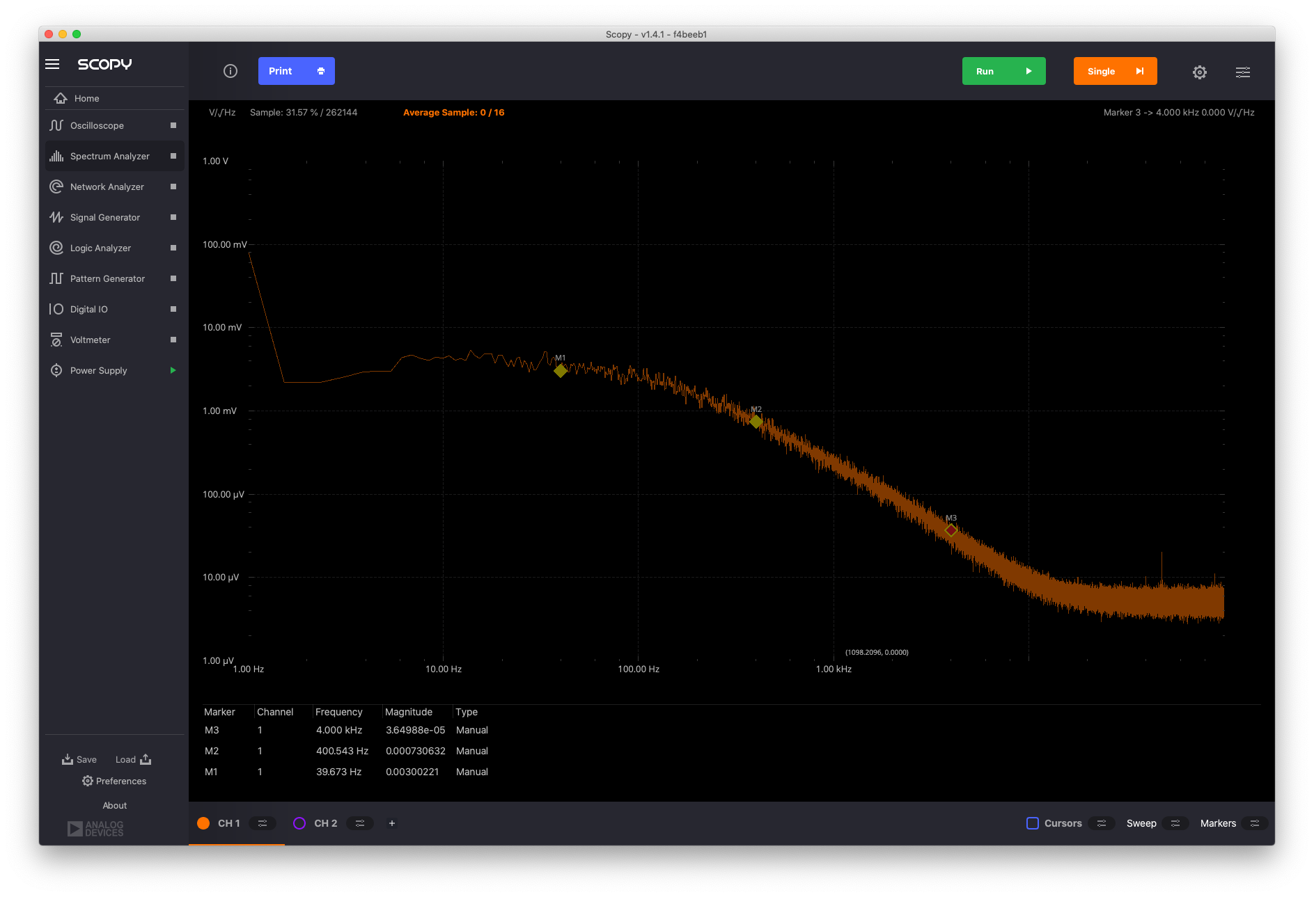
Fig. 2.43 The output of the OTA when placed in DC feedback but AC open loop; we observe the spectrum of the output noise of the OTA#
This requires further analysis, but a rough analysis indicates that the noise is dominated by 1/f noise.
To Do#
Show the effect of zero compensation resistor
take unity-gain case since phase margin is largest there
Look at scaling of the step responses with amplitude via csv files
Investigate the difference between the two frequency domain results
combine the frequency domain csv files
does this have anything to do with the input signal attenuator
or the feedback resistor value
Why are the DC sweeps off?
Do an inverting configuration
Lower frequency –> fu of 100KHz
More comparison to simulation
Non-linearity measurements – distortion