3.1.5. Lab 5: One-stage OTA and Common-Source Amplifier#
Objective#
In this experiment we measure the frequency response of a one-stage operational transconductance amplifier (OTA) and a common-source (CS) amplifier. Based on the measured performance, we build behavioral models of the amplifiers. In later labs we will combine these stages into a two-stage OTA that requires compensation.
Preparation#
Review your course notes on one-stage OTAs and CS stages.
Review the experiments below and build up an understanding of what you should observe in the measurements. You can consider doing some circuit simulations to get familiar with the biasing and the operation of the amplifiers.
Review the chip schematic and pin map to find where the relevant components are. In this lab we will use the pMOS one-stage OTA and the 4x nMOS CS transistor and the pMOS current mirror.
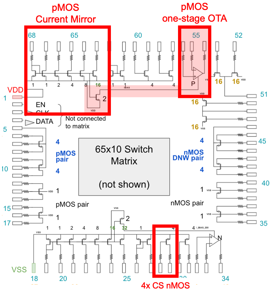
Fig. 3.6 Schematic of the MOSbius chip with one-stage pMOS OTA, the 4x CS transistor and the pMOS current mirror highlighted#
Materials#
MOSbius Chip & PCB
Breadboard & Wires
Resistors: \(100\Omega\) (two), \(100K\Omega\) (two)e
Signal Capacitors: \(470pF\), \(47nF\) and \(4.7nF\) or values that are close;
Bias Capacitors: \(47\mu F\) electrolytic and \(1\mu F\) non-electrolytic
Potentiometer: \(25K\Omega\)
ADALM2000 Active Learning Module (DC Power Supply, Oscilloscope, Waveform Generator, Network Analyzer)
Experiments#
The frequency response of the two amplifiers is measured to determine their small-signal performance parameters like DC gain, bandwidth, unity-gain frequency; then the small-signal parameter of the amplifier’s behavioral model are determined, including the \(g_m\), \(R_{out}\), and \(C_{out}\). Appropriate external load capacitors are used to assure that the parasitics do not significantly affect the performance.
Single-Stage pMOS OTA#
Build the Test Circuit and Check the Bias Point#

Fig. 3.7 Schematic of the one-stage pMOS OTA with a 2x \(I_{REF}\) current bias. The OTA is loaded with \(C_{L1}\) and is placed in negative DC feedback with \(R_2\), \(R_1\) and \(C_{B1}\) and in AC feedback with \(R_2\), \(R_1\). The biasing of the input pin is not shown.#
Build the test circuit:
The pMOS current mirror is biased using the 25K potentiometer provided on the PCB (close to I_REFP). Connect a current meter across I_REFP with the positive lead on the left and the negative lead on the right side of the header; adjust the potentiometer so \(I_{REF}\) is \(100\mu A\); replace the current meter with a jumper. The I_REFP header is connected to pin 68 of the MOSbius chip on the PCB. See Testing the Current Bias Potentiometers in the Appendix on Testing the MOSbius PCB
The OTA is internally connected to the current mirror with a 2X tail transistor M7 so it is biased with \(200\mu A\).
Use a \(470pF\) capacitor as \(C_{L1}\).
Use \(R_1 = 100\Omega\) and \(R_2 = 100K\Omega\) and \(C_{B1} = 47\mu F\).
Use the \(25K\Omega\) potentiometer (or similar) to generate a \(1.25V\) reference voltage \(V_{REF}\) and decouple it with the \(1\mu F\) capacitor \(C_{REF}\) (or similar).
Understand the operation of the OTA in the test circuit:
Draw a DC equivalent for the circuit and prove to yourself that the OTA is in negative, series-shunt feedback with unity gain for DC (\(\beta = 1\)).
Draw an AC equivalent for the circuit and prove to yourself that the OTA is in negative, series-shunt feedback with a feedback factor \(\beta\) of \(R_1/(R_1+R_2) = 1/1,001\) for AC signals.
Study for which frequencies the OTA will be in AC feedback, i.e. where \(\beta = R_1/(R_1+R_2)\).
What would happen if we connected \(R_1\) to \(V_{REF}\) directly instead of to \(C_{B1}\). (Hint: The OTA has a DC offset.)
Verify the DC bias point:
Apply the 2.5V power supply to the chip and short in to \(V_{REF}\).
Measure and record the various DC node voltages[1]: inn, inp (= in), out.
Review that the voltages make sense.
If there is a voltage difference between out and inn, then likely there is leakage through \(C_{B1}\); replace it with a non-electrolytic (possibly smaller) capacitor.
Oscilloscope Measurements#
We start with measurements on the oscilloscope at low frequencies to determine an appropriate input amplitude for the network analyzer measurements. We will also obtain a first estimate of the gains and these measurements can be used to do a sanity check on our network analyzer measurements later.
Gain:
Generate a \(1KHz\) \(50mV_{pp}\) sine wave with a \(1.25V\) DC offset with W1. Always disconnect the signal generator first and verify the signal on the oscilloscope before applying it to your circuit. Do not apply signals above \(2.5V\) or below \(0V\) to the chip
Disconnect in from \(V_{REF}\) and connect it to the signal generator W1.
Connect the oscilloscope channels 1+ and 2+ to in and out respectively and ground 1- and 2-.
Measure the waveforms at input and output and record the amplitudes.
Estimate the gain of the amplifier \(A=\frac{V_{out,pp}}{V_{in,pp}}\).
Repeat with a \(25mV_{pp}\) and \(100mV_{pp}\) and check that the OTA operates in its linear range for an input of \(50mV_{pp}\).
Network Analyzer Measurements#
Gain vs Frequency:
Set up the Network Analyzer to use channel 1 as the reference and channel 2 as the output. Make sure to specify a signal with a 1.25V offset and \(25mV\) amplitude[2]. Turn on DC filtering at set the settling times to \(40ms\). Ten periods and 10 averages typically give good results. Turn on the scope view during NA measurements to verify the correct operation of the amplifier. Adjust the NA settings if needed.
Measure the \(A=\frac{V_{out}}{V_{in}}\) between \(100Hz\) and \(1MHz\) using e.g. 200 points.
Can you determine the open-loop, LF gain of the OTA? What is an appropriate frequency to measure it?
Can you determine the frequency \(f_1\) of the dominant pole of the OTA’s open-loop frequency response?
Does the OTA have higher-order poles?
What is the unity-gain frequency \(f_u\) of the OTA in open loop?
Explain why you are measuring the open-loop performance of the OTA even though there is a feedback network around the OTA.
Remove \(C_{L1}\) and repeat the frequency response measurement.
Compare the results and confirm that \(C_{L1} = 470pF\) dominates over the parasitics.
OTA Behavioral Model#
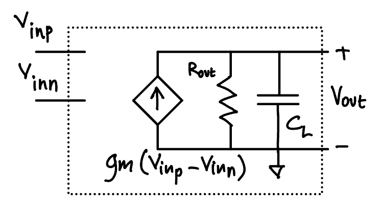
Fig. 3.8 Schematic for the OTA behavioral model#
Build an equivalent behavioral model of the OTA
Check the expressions for \(f_u\) and \(f_1\) and find \(g_m\) and \(r_{out}\) from the measurements, assuming that \(C_{L1}\) is significantly larger than any circuit, chip or breadboard parasitics.
Estimate the \((g_m/I_{DS})\) of the differential-pair input transistors.
4x nMOS Common-Source Amplifier#
Build the Test Circuit and Check the Bias Point#

Fig. 3.9 Schematic of the 4x common-source nMOS amplifier. M5 is biased a 4x \(I_{REF}\) current bias and its DC gate voltage is generated with DC OTA feedback.#
Build the test circuit:
The pMOS current mirror is biased as before.
The 4x nMOS M5 is placed in a common-source configuration and biased with the 4x pMOS current-mirror transistor M6.
Use a \(4.7nF\) capacitor as \(C_{L2}\).
Use \(R_{B2} = 100K\Omega\), \(C_{B2} = 47nF\) and \(C_{B3} = 1\mu F\).
Use the \(25K\Omega\) potentiometer (or similar) to generate a \(1.25V\) reference voltage \(V_{REF}\) and decouple it with a \(1\mu F\) capacitor \(C_{REF}\) (or similar).
Understand the operation of the CS amplifier in the test circuit:
Draw a DC equivalent for the circuit and prove to yourself that the OTA generates the appropriate \(V_{GS,5}\) so that \(V_{DS,5} = 1.25V\) and \(I_{DS,5} = 400\mu A\).
Draw an AC equivalent for the circuit and prove to yourself that M5 amplifies the AC signal from in to out. Determine for which frequencies this happens.
Verify the DC bias point:
Apply the 2.5V power supply to the chip.
Measure and record the various DC node voltages[1]: out, OTAout, \(V_{GS,5}\).
Review that the voltages make sense.
Oscilloscope Measurements#
We start again with measurements on the oscilloscope at low frequencies to determine an appropriate input amplitude for the network analyzer measurements. We will also obtain a first estimate of the gains and these measurements can be used to do a sanity check on our network analyzer measurements later.
Gain:
Generate a \(1KHz\) \(20mV_{pp}\) sine wave with a \(0V\) DC offset with W1. Always disconnect the signal generator first and verify the signal on the oscilloscope before applying it to your circuit. Do not apply signals above \(2.5V\) or below \(0V\) to the chip
Connect in to the signal generator W1.
Connect the oscilloscope channels 1+ and 2+ to in and out respectively and ground 1- and 2-.
Measure the waveforms at input and output and record the amplitudes.
Estimate the gain of the amplifier \(A=\frac{V_{out,pp}}{V_{in,pp}}\).
Repeat with a \(10mV_{pp}\) and \(30mV_{pp}\) and check that the OTA operates in its linear range for an input of \(20mV_{pp}\).
Network Analyzer Measurements#
Gain vs Frequency:
Set up the Network Analyzer to use channel 1 as the reference and channel 2 as the output. Make sure to specify a signal with a 0V offset and \(20mV\) amplitude[2]. Turn on DC filtering at set the settling times to \(40ms\). Ten periods and 10 averages typically give good results. Turn on the scope view during NA measurements to verify the correct operation of the amplifier. Adjust the NA settings if needed.
Measure the \(A=\frac{V_{out}}{V_{in}}\) between \(100Hz\) and \(1MHz\) using e.g. 200 points.
Can you determine the LF gain of the CS amplifier? What is an appropriate frequency to measure it?
Can you determine the frequency \(f_1\) of the dominant pole of the CS amplifier’s frequency response?
Are there higher-order poles?
What is the unity-gain frequency \(f_u\) of the CS amplifier’s frequency response?
Remove \(C_{L2}\) and repeat the frequency response measurement
Compare the results and confirm that \(C_{L2} = 4.7nF\) dominates over the parasitics.
CS Amplifier Behavioral Model#
Build an equivalent behavioral model of the CS amplifier
Check the expressions for \(f_u\) and \(f_1\) and find \(g_m\) and \(r_{out}\) from the measurements, assuming that \(C_{L2}\) is significantly larger than any circuit, chip or breadboard parasitics.
Estimate the \((g_m/I_{DS})\) of the CS transistor.
What possible effect does the OTA feedback DC bias have on your measurements?
Suggestions#
Run simulations of the experiments to gain insight in the circuit behavior. Note that simulations, measurements and calculations can differ due to the presence of parasitic capacitors on the chip and breadboard. However, we are using large capacitors in these experiments so that the effect of parasitic capacitors should be minimal.
Double the bias current on the one-stage OTA and the CS amplifier and observe the change in performance.
Change the values of \(C_{L1}\) and \(C_{L2}\) and check that you get consistent estimates for \(g_{m}\) based on the measured unity-gain frequencies \(f_u\).