3.1.4. Lab 4: Differential Pair AC Response#
Attention
There are a lot of experiments, it is OK if you cannot finish them all. Do them in the order listed below.
Objective#
In this experiment, you will learn about differential signals and circuits through building and characterizing a differential pair. The differential pair amplifies differential input signals but rejects common-mode input signals. We will focus on the differential-mode and common-mode responses w.r.t. frequency.
Preparation#
Review your course notes on differential signals and the theory of the operation of the differential pair.
Review the experiments below and build up an understanding of what you should observe in the measurements. You can consider doing some circuit simulations to get familiar with the DC operation of a differential pair.
Review the chip schematic and pin map to find where the relevant components are. In this lab we will use the 4x nMOS transistors and the nMOS current mirrors to build an nMOS differential pair.
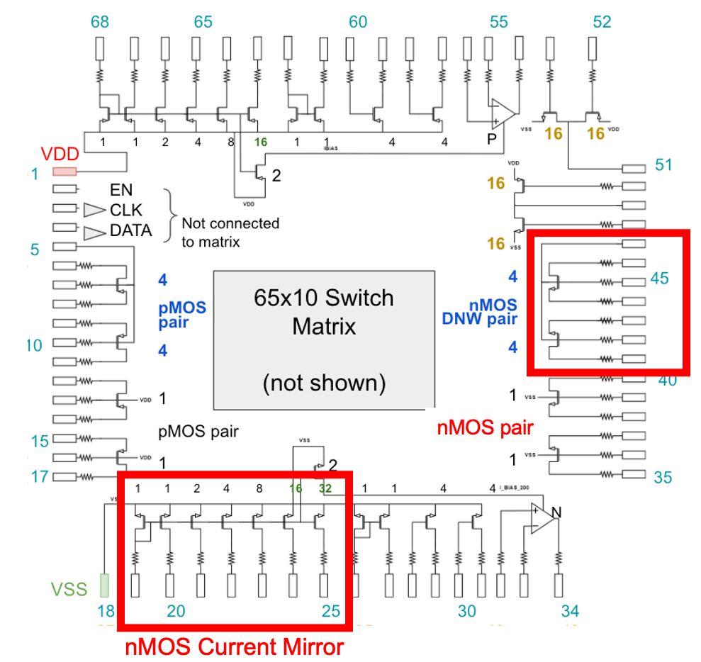
Fig. 3.3 Schematic of the MOSbius chip with the nMOS current mirror and the 4x nMOS differential-pair transistors highlighted#
Materials#
MOSbius Chip & PCB
Breadboard & Wires
Resistors: \(4.7K\Omega\) (eight) or \(1.2K\Omega\) (two)
Capacitors: \(1.2nF\) (two) and \(8.2nF\) or values that are close; \(1\mu F\) (or similar large decoupling capacitor)
Potentiometer: \(25K\Omega\)
ADALM2000 Active Learning Module (DC Power Supply, Oscilloscope, Waveform Generator, Network Analyzer)
Experiments#
The experiments start with measuring the differential amplifier in a typical use case where \(C_{CS}\) is as small as possible, so we add no \(C_{CS}\) to the circuit.
Next we will explore the effect of the \(C_{CS}\) capacitor on the common-mode response, which will offer a lot of insight in how the differential pair responds to common-mode versus differential-mode signals.
Finally we will study the difference between a differential load capacitor and two single-ended load capacitors.
In these experiments we will drive one input of the differential amplifier with a single-ended signal source[1] and will connect the other input with a bias voltage. We will observe that this applies both a differential-mode and common-mode signal to the amplifier.
Build the Circuit and Check the Bias Point#

Fig. 3.4 Schematic of the nMOS differential pair with a 8x \(I_{REF}\) current bias. Note the location of the load capacitors \(C_L\) and the common-source capacitor \(C_{CS}\). The capacitors will not always be used for all parts of the experiments. The biasing of the input pins is not shown.#
Build the circuit:
The current mirror is biased using the 25K potentiometer provided on the PCB (close to I_REFN). Connect a current meter across I_REFN with the positive lead on the left and the negative lead on the right side of the header; adjust the potentiometer so \(I_{REF}\) is \(100\mu A\); replace the current meter with a jumper. The I_REFN header is connected to pin 19 of the MOSbius chip on the PCB. See Testing the Current Bias Potentiometers in the Appendix on Testing the MOSbius PCB
Use the 8x output of the current mirror to bias the differential pair. So each transistor[2] is biased with \(400\mu A\).
The body[3] of transistors M1 and M2 needs to be connected to GND (VSS).
Place the load resistors \(R_L\) of \(\frac{4.7K\Omega}{4}\) or equivalent on the breadboard. Measure your resistors with a multimeter and note their values. Ideally the two loads should be identical.
Use the \(25K\Omega\) potentiometer (or similar) to generate a \(1.25V\) reference voltage \(V_{REF}\) and decouple it with the \(1\mu F\) capacitor \(C_{REF}\) (or similar).
Verify the DC bias point:
Apply the 2.5V power supply to the chip and short INp and INn to \(V_{REF}\).
Measure and record the various node voltages.
Review that the voltages make sense; e.g., estimate the currents through M1 and M2 by looking at the voltage drop across the \(R_L\) resistors; check the \(V_{GS}\) of M1, M2, MCM1; check the \(V_{DS}\) of MCM2.
Standard Operation \(C_{CS}=0\)#
Oscilloscope Measurements#
We start with measurements on the oscilloscope at low frequencies to determine an appropriate input amplitude for the network analyzer measurements. We will also obtain a first estimate of the gains and these measurements can be used to do a sanity check on our network analyzer measurements later. Preferably we also want to null the DC offset at the output.
Nulling the offset:
Connect the signal generator W1 to INp and \(V_{REF}\) to INn.
Generate a constant 1.25V voltage with the signal generator W1.
Observe \(V_{OUTn}\) and \(V_{OUTp}\); there will likely be a DC offset; adjust \(V_{REF}\) to minimize the output offset. Measure and note the new \(V_{REF}\) and make sure its value is reasonable.
Differential Gain:
Generate a 300Hz 200mVpp sinewave with a 1.25V DC offset with W1. Always disconnect the signal generator first and verify the signal on the oscilloscope before applying it to your circuit. Do not apply signals above \(2.5V\) or below \(0V\) to the chip
Connect the oscilloscope channels 1+ and 2+ to the two outputs and ground 1- and 2-.
Create two mathematical channels[4] in the oscilloscope, namely the differential mode, \(V_{OUTp}-V_{OUTn}\), and the common mode, \((V_{OUTp}+V_{OUTn})/2\), and turn on the measurements.
Measure the waveforms at the outputs and record the amplitudes. The mathematical channels will very helpful here.
Estimate the differential gain of the amplifier \(A_{dd} = \frac{V_{OUTp}-V_{OUTn}}{V_{INp}-V_{INn}}\).
Given you know \(R_L\), estimate the \(g_m\) of M1 and M2 and their \((g_m/I_{DS})\).
Repeat with a 100mVpp and 300mVpp sinewave and check that the differential amplifier operates in its linear range for an input of 200mVpp.
Common-Mode Gain:
Disconnect \(V_{INn}\) from \(V_{REF}\) and short it to \(V_{INp}\) which is connected to the signal generator W1.
Measure the waveforms at the outputs.
Estimate the common-mode gain of the amplifier \(A_{cc} = \frac{V_{OUTp}+V_{OUTn}}{V_{INp}+V_{INn}}\).
Knowing \(R_L\) can you estimate the output impedance of the current source transistor MCM2?
Network Analyzer Measurements#
Differential Gain vs Frequency:
Put the circuit back in the differential-mode configuration: connect the signal generator to \(V_{INp}\) and \(V_{REF}\) to \(V_{INn}\).
Connect oscilloscope channel 1 across the input, i.e. 1+ to \(V_{INp}\) and 1- to \(V_{INn}\), and channel 2 across the output, i.e. 2+ to \(V_{OUTp}\) and 2- to \(V_{OUTn}\).
Set up the Network Analyzer to use channel 1 as the reference and channel 2 as the output. Make sure to specify a signal with a 1.25V offset and 100mV amplitude[5]. Turn on DC filtering at set the settling times to \(20ms\). Increase the number of periods and averages if needed. Ten periods and 10 averages typically gives good results.
Measure the \(A_{dd}\) between \(100Hz\) and \(10MHz\) using e.g. 200 points.
Measure and compare the gain and bandwidth for \(C_L\) is \(0\) and \(1.2nF\). How do the results compare to your estimates and to the oscilloscope measurements.
Common-Mode Gain vs Frequency:
Put the circuit in the common-mode measurement configuration: connect the signal generator to \(V_{INp}\) and short \(V_{INp}\) and \(V_{INn}\).
Connect oscilloscope channel 1 between \(V_{INp}\) and GND and oscilloscope channel 2 between \(V_{OUTn}\) and GND.
Measure the \(A_{cc}\) between \(100Hz\) and \(10MHz\).
Measure and compare the gain and bandwidth for \(C_L\) is \(0\) and \(1.2nF\). How do the results compare to your estimates and to the oscilloscope measurements.
Response at the Common Source:
Keep the circuit in the common-mode configuration.
Measure the \(V_{CMSRC}\) vs \(V_{IN}\). Can you explain the responses? Note that you are now basically measuring a source follower (assuming that the \(R_L\) have a negligible effect, which is the case).
Common-Mode Rejection Ratio:
Measure \(A_{dd}\), take a snapshot (and save the trace if you want to do post processing), and then measure \(A_{cc}\) and compare; their ratio is often referred to as the common-mode-rejection ratio \(CMRR = \frac{A_{dd}}{A_{cc}}\); do this for the following capacitor combinations:
\(C_L = 1.2nF\) and \(C_{CS} = 0\)
Discuss the CMRR vs frequency.
Warning
Next we are going to add a large capacitor from the CMSRC node to GND. In actual design this is NOT recommended. We do this here for educational purposes so you can learn about the effect of capacitance at the CMSRC node.
Studying the Effect of \(C_{CS}\)#
Keep \(C_L = 1.2nF\) and add a \(C_{CS}\) of \(8.2nF\)
Repeat the \(A_{dd}\) measurements.
Are there any differences? Explain.
Repeat the \(A_{cc}\) measurements.
Are there any differences? Explain.
Repeat the measurement of the response at the common source.
Can you correlate what you observe to what you observe for \(A_{cc}\)?
Discuss the CMRR vs. frequency.
Differential Load Capacitors vs Single-Ended Load Capacitors#
Fig. 3.5 Schematic of the nMOS differential pair with a 8x \(I_{REF}\) current bias. Note the different configuration for the load capacitors \(C_L\). Their common point needs to be floating.#
Differential Load:
Measure \(A_{dd}\) and \(A_{cc}\) with load capacitors connected as shown in the figure above and with \(C_{CS}=0\). Discuss the CMRR vs. frequency.
Now do an oscilloscope measurement for a 1MHz input signal and observe the various nodes. Can you explain what you observe?
You can repeat for \(C_{CS}=8.2nF\).
Suggestions#
Run simulations of the experiments to gain insight in the circuit behavior. Note that simulations, measurements and calculations can differ due to the presence of parasitic capacitors on the chip and breadboard. However, we are using large capacitors in these experiments so that the effect of parasitic capacitors should be minimal.