10.1. Testing Your MOSbius PCB#
10.1.1. Review the PCB Description#
Read the PCB Description. Note all the GND are connected on the PCB and are connected to the - power rail terminal.
10.1.2. Visually Inspect the PCB#
Preferably under a microscope or using a magnifier glass (e.g., use the magnifier glass app on your phone), inspect the PCB and verify that all components are properly soldered to the pads and that there are no ‘cold’ solder joints.
10.1.3. Remove the MOSbius Chip#
Start your tests without a MOSbius chip in the socket. When removing the chip, make sure that your use ESD safe practices. Use an ESD grounding strap. Store the chip in a ESD safe container after removing it from the PCB.
10.1.4. Plug Your PCB in a Solderless Breadboard#
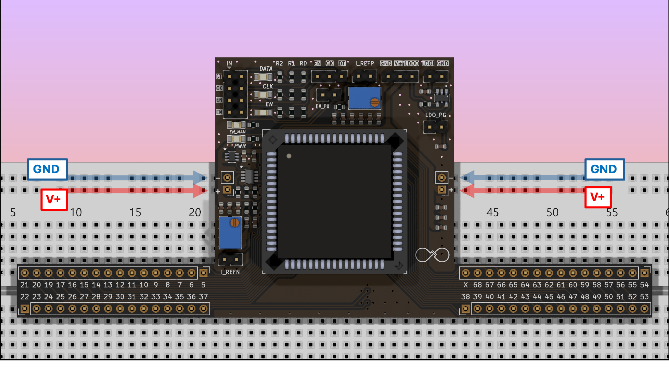
Make sure to orient your PCB correctly so that the top power rail is GND (or VSS) (typically colored blue) and the power rail below is VDD (typically colored red).
Push the PCB down and make sure that all pins are inserted properly, including the VDD/VSS pins on top.
10.1.5. Testing the Power Supply and Supply Protection#
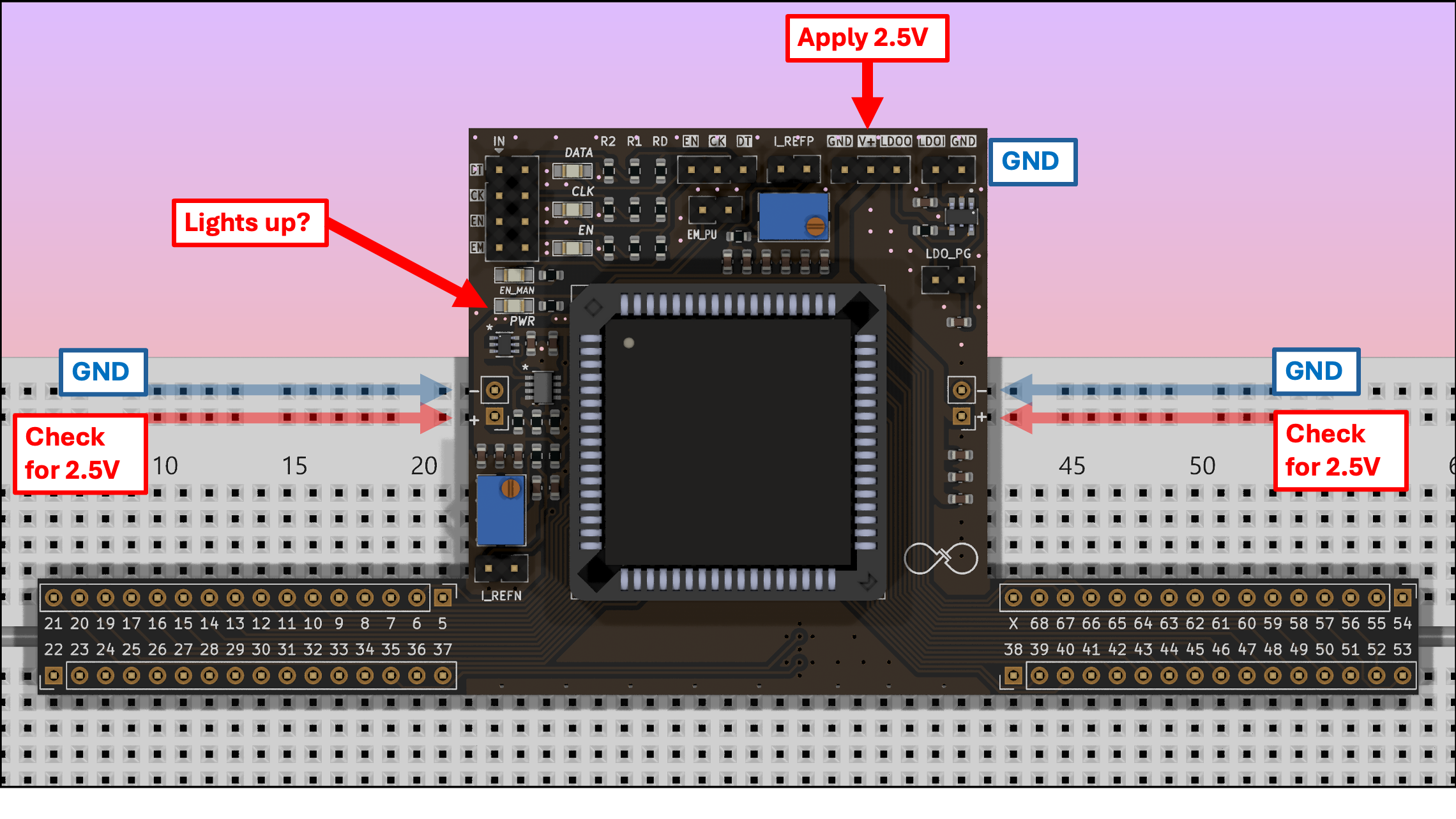
Apply 2.5V to
V+and verify that the redPWRLED lights up; verify that the 2.5V voltage appears on the solderless breadboard power rail. Once this works you can choose to connect your external 2.5V power supply to the breadboard or theV+terminal.Increase the supply voltage beyond 2.5V and verify that the
PWRLED goes off; the protection circuit should cut the power to the chip.
10.1.6. Testing the Digital Level Shifters#
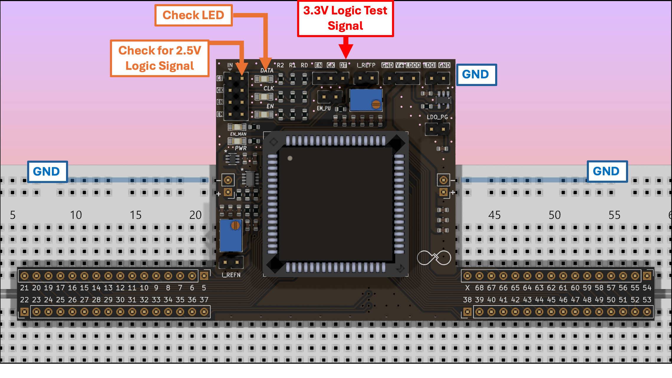
Apply a 3.3V logic signal, e.g. a clock, to the data
DTterminal on the top of the PCB. The blueDATALED should light up or flicker, depending on the frequency you use. Make sure to properly connect the ground between the PCB and your signal source.Using a scope, verify that the signal on the header is reduced in voltage to a 2.5V logic signal.
(not shown) Repeat this for the clock
CK(yellowCLKLED) and the enableEN(greenENLED).
10.1.7. Testing the Manual Enable#
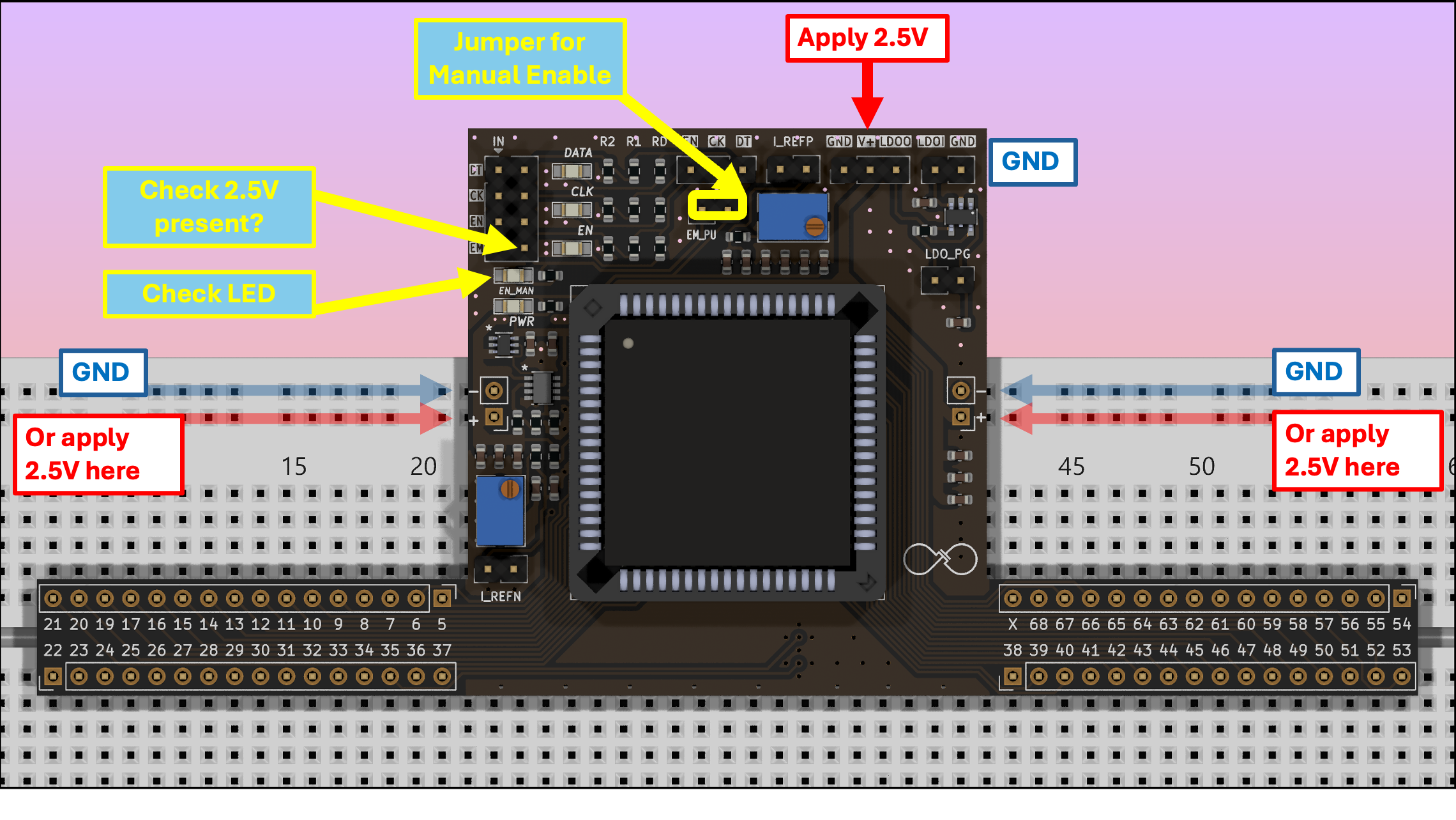
Put a jumper on the
EM_PUheader and verify that theEMsignal is 2.5V and that the orangeEN_MANLED ligths up.
10.1.8. Connecting the Logic Signals#
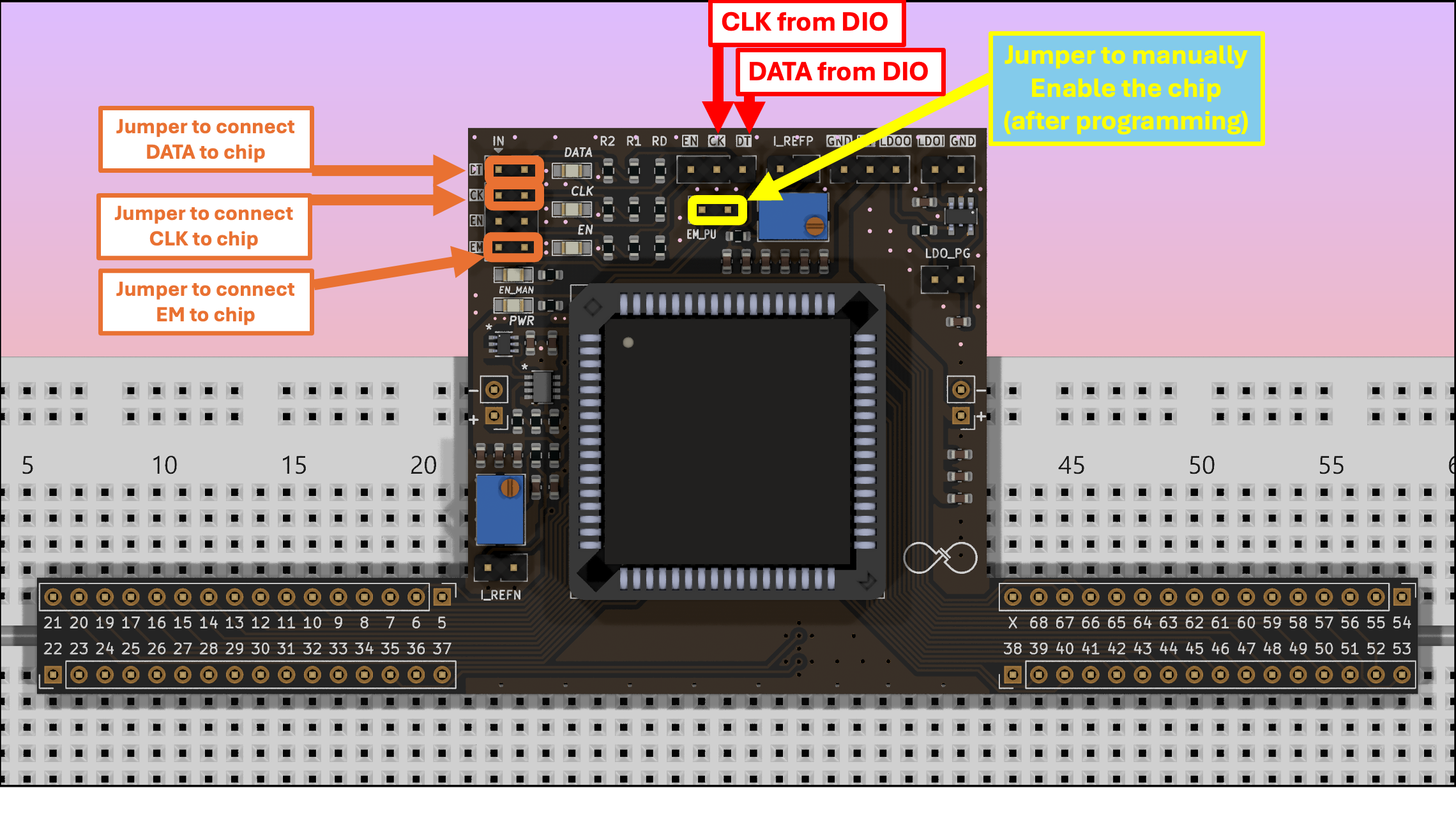
You can now place jumpers to connect the logic signals to the chip. Figure shows the case for using the manual enable. See Programming the Chip.
10.1.9. Testing the LDO#
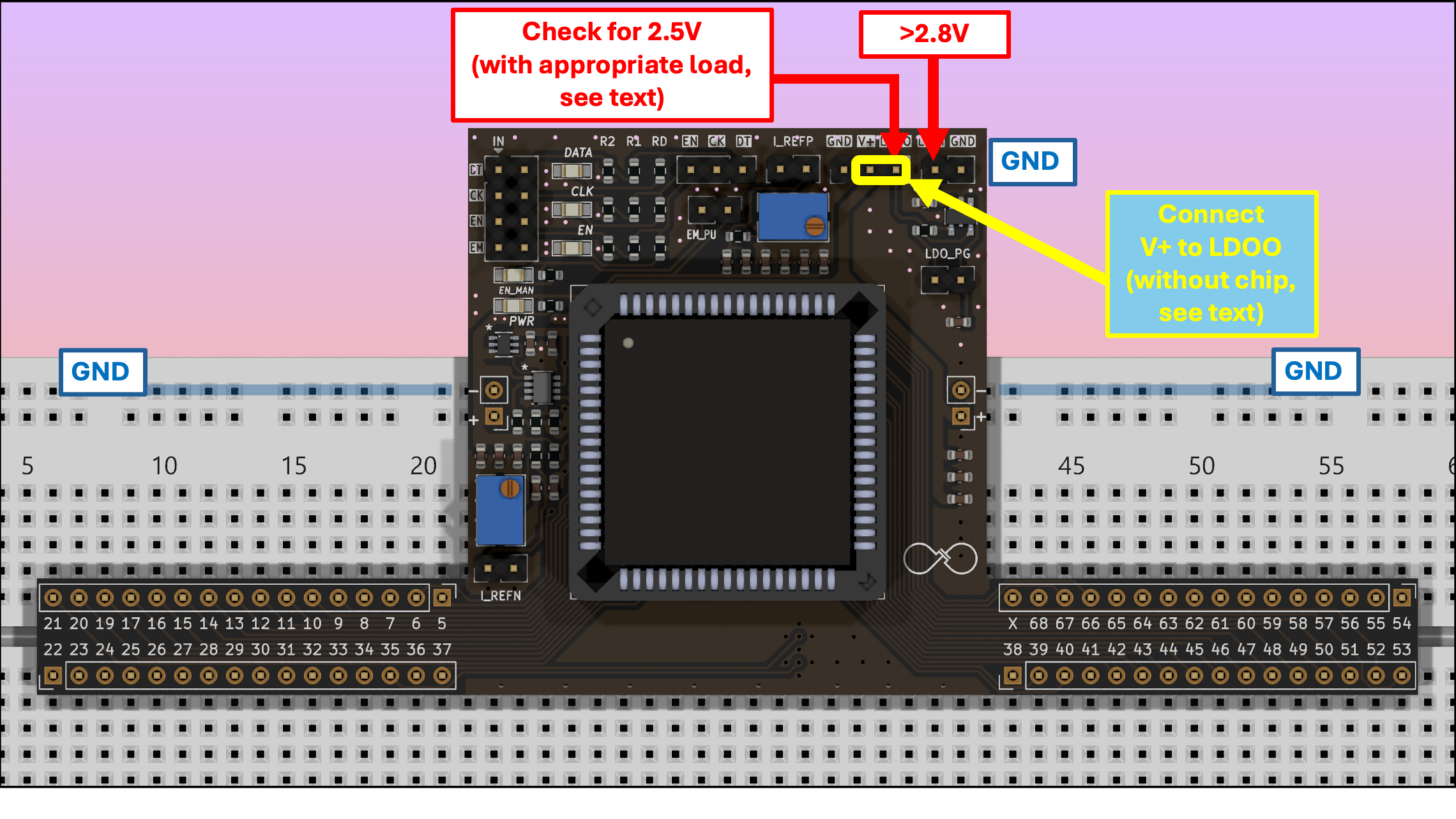
If you plan to use an external power supply that is higher than 2.5V, you can the LDO to regulate the supply to 2.5V.
Apply 3.3V between
LDOIandGND. No capacitive load is connected to theLDOOand it will not properly stabilize.If no chip is in the socket, you can place a jumper between
LDOOandV+and use the PCB supply decoupling caps to load and stabilize theLDOO. Measure theV+waveform with a scope to verify that it is 2.5V and noise and ripple free.If you have a chip in the socket, do not connect
LDOOtoV+, but connect an external \(1\mu F\) capacitor betweenLDOOandGND(e.g. on a spare node the breadboard). Measure theLDOOwaveform with a scope to verify that it is 2.5V and noise and ripple free. If so, you can remove the external capacitor and place a jumper betweenLDOOandV+.
Typically not required: If you connect a jumper on the LDO power good signal LDO_PG, it will go to the LDOI level if the LDO is operating properly. For most uses of the PCD you will not need this.
10.1.10. Insert MOSbius Chip#
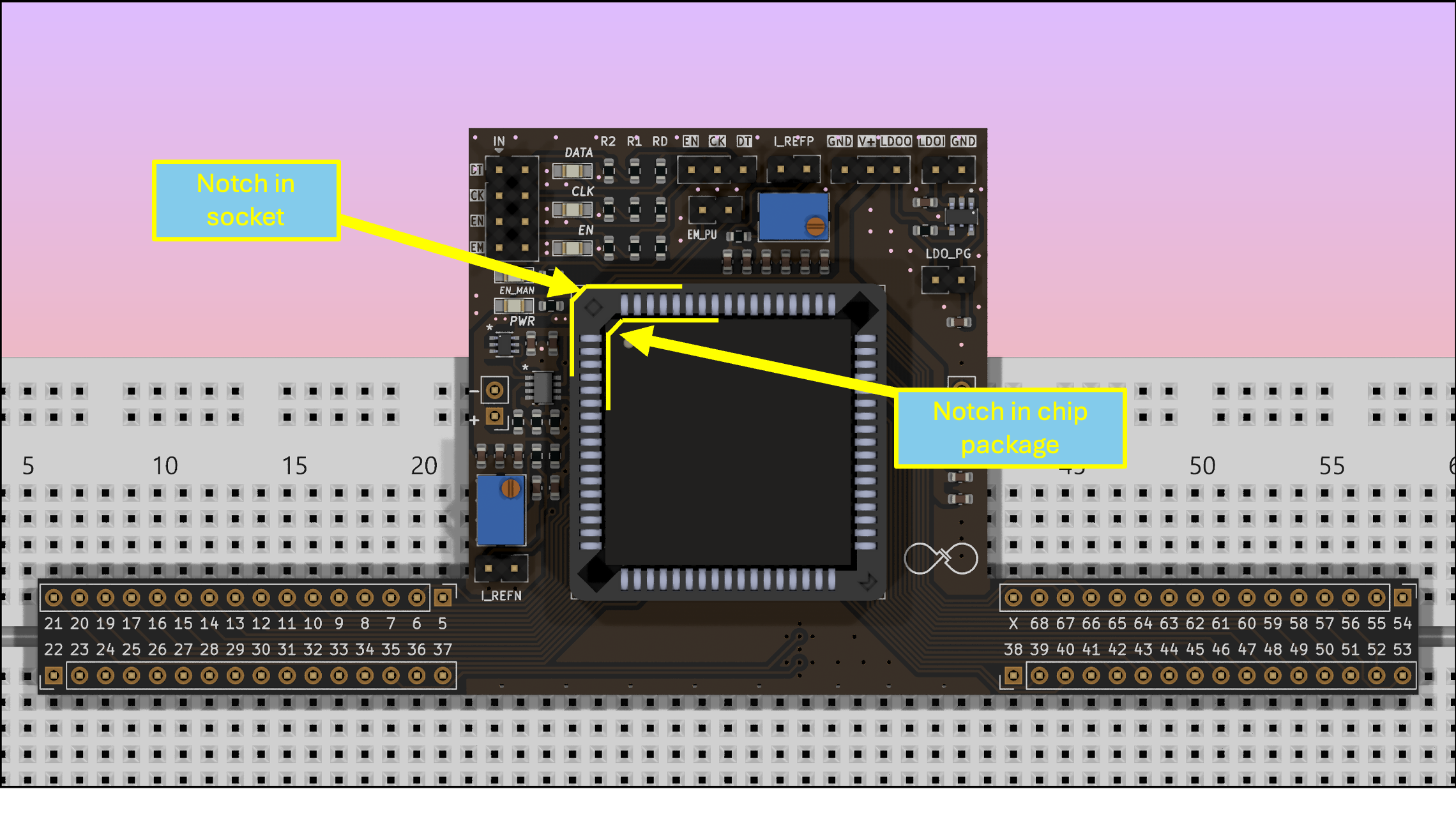
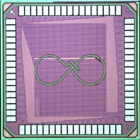
Verify that the socket is correctly soldered on the PCB. Pin 1 is in the upper left corner.
Insert a chip in the socket. Normally the chip only fits one way in the socket. Verify that the chip is seated properly.
10.1.11. Testing the Current Bias Potentiometers#
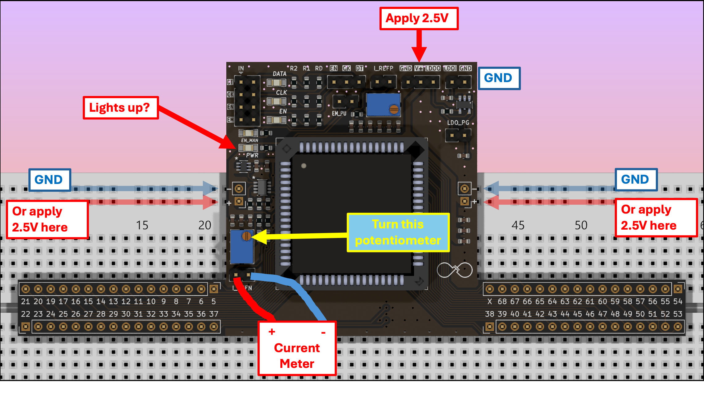
nMOS: Connect a current meter at the
I_REFNterminal. You should measure a current of tens of microamperes. Turn the potentiometer and verify that you can change the current bias. A typical current bias is \(100\mu A\) so you can set it to this value for now.
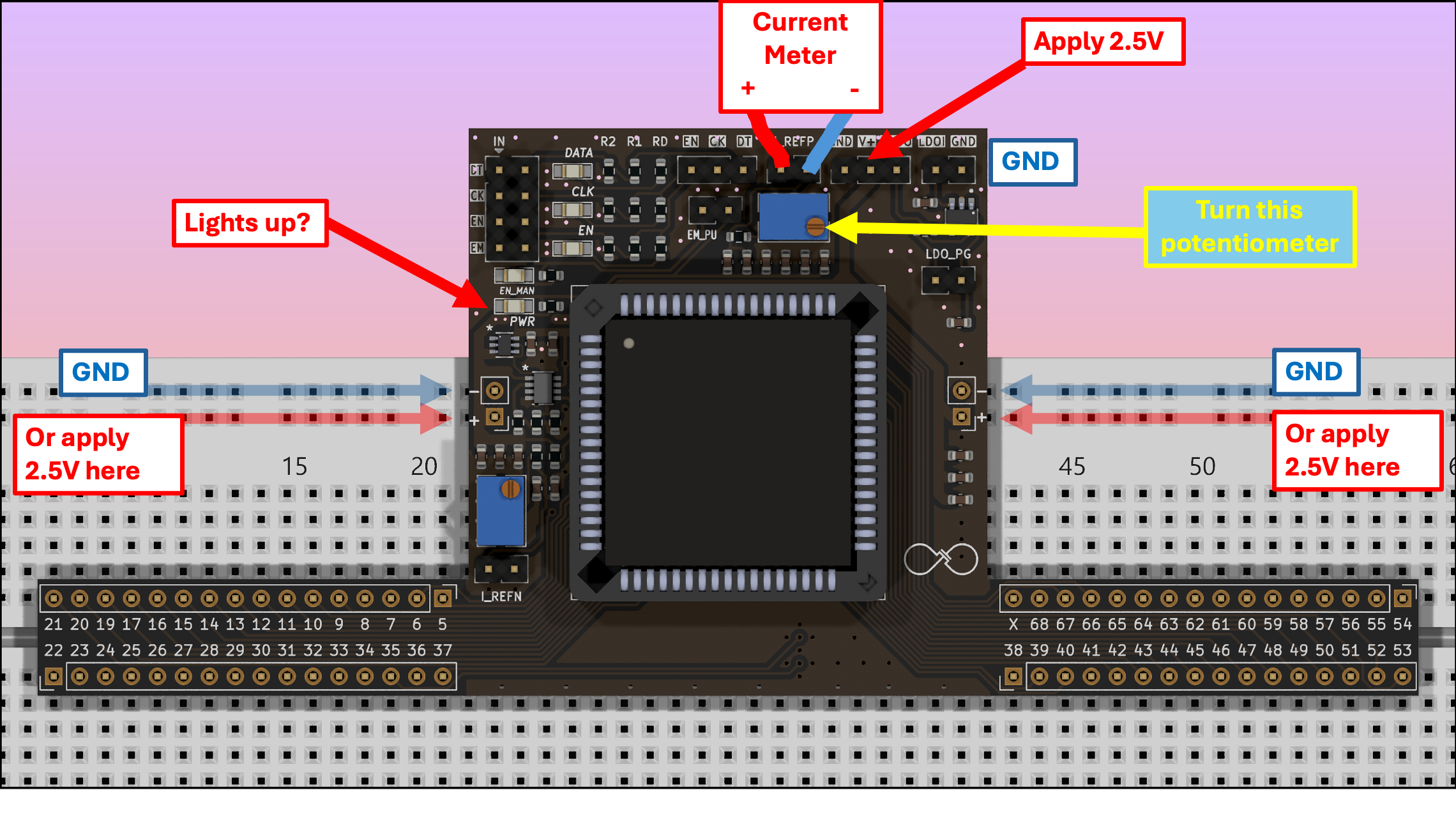
pMOS: Similarly, connect a current meter at the
I_REFPterminal. You should measure a current of tens of microamperes. Turn the potentiometer and verify that you can change the current bias. A typical current bias is \(100\mu A\) so you can set it to this value for now.
10.1.12. Ready, Start, Experiment!#
Your PCB is now ready to use for your MOS circuits exploration. Have fun!