3.1.3. Lab 3: Differential Pair DC Response#
Attention
There are a lot of experiments, it is OK if you cannot finish them all. Do them in the order listed below. It is OK if you cannot complete the experiments with different bias conditions and the subsequent experiments.
Objective#
In this experiment, you will learn about differential signals and circuits through building and characterizing a differential pair. The differential pair amplifies differential input signals but rejects common-mode input signals. We will focus on the DC responses.
Preparation#
Review your course notes on differential signals and the theory of the operation of the differential pair.
Review the experiments below and build up an understanding of what you should observe in the measurements. You can consider doing some circuit simulations to get familiar with the DC operation of a differential pair.
Review the chip schematic and pin map to find where the relevant components are. In this lab we will use the 4x nMOS transistors and the nMOS current mirrors to build an nMOS differential pair.
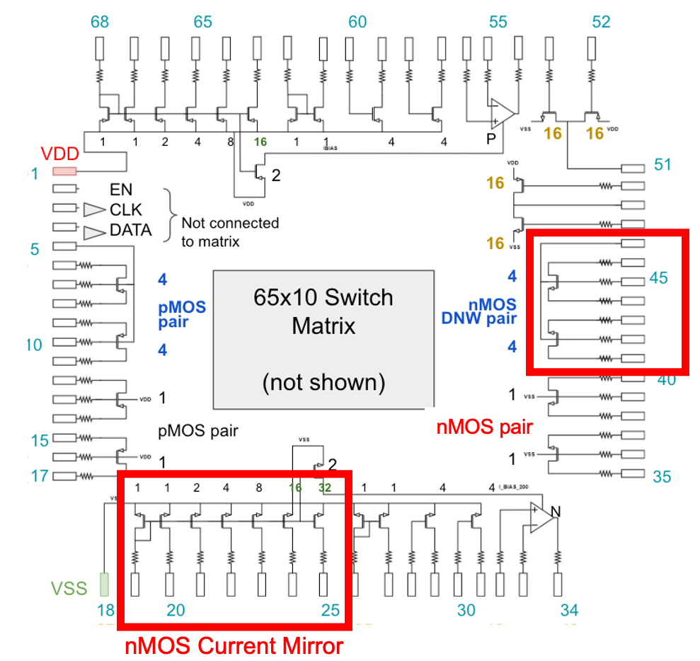
Fig. 3.1 Schematic of the MOSbius chip with the nMOS current mirror and the 4x nMOS differential-pair transistors highlighted#
Materials#
MOSbius Chip & PCB
Breadboard & Wires
Resistors: \(4.7K\Omega\) (several)
ADALM2000 Active Learning Module (DC Power Supply, Oscilloscope, Waveform Generator)
Experiments#
Build the Circuit and Check the Bias Point#

Fig. 3.2 Schematic of the nMOS differential pair with a 2x \(I_{REF}\) current bias#
The current mirror is biased using the 25K potentiometer provided on the PCB (close to I_REFN). Connect a current meter across I_REFN with the positive lead on the left and the negative lead on the right side of the header; adjust the potentiometer so \(I_{REF}\) is \(100\mu A\); replace the current meter with a jumper. The I_REFN header is connected to pin 19 of the MOSbius chip on the PCB. See Testing the Current Bias Potentiometers in the Appendix on Testing the MOSbius PCB
For the initial experiments use the 2x output of the current mirror to bias the differential pair. So each transistor is biased with \(100\mu A\). Note that you will change this in later experiments.
The body[1] of transistors M1 and M2 needs to be connected to GND (VSS).
Place the load resistors \(R_L\) on your breadboard. For the initial experiments \(R_L\) is \(4.7K\Omega\). Measure your resistors with a multimeter and note their values. Ideally the two resistors should be identical.
Verify the DC bias point:
Apply the 2.5V power supply to the chip and bias INp and INn with \(1.25V\).
Measure and record the various node voltages.
Review that the voltages make sense; e.g., estimate the currents through M1 and M2 by looking at the voltage drop across the \(R_L\) resistors; check the \(V_{GS}\) of M1, M2, MCM1; check the \(V_{DS}\) of MCM2.
Measure the DC Common-Mode Response#
Tie the inputs INp and INn together and apply a \(100Hz\) triangle wave with a DC bias of \(1.25V\) and a peak-to-peak amplitude of \(2.5Vpp\) as the common-mode input \(V_{CM}\). Verify the common-mode signal on the oscilloscope before applying it to your circuit. Do not apply signals above \(2.5V\) or below \(0V\) to the chip
Measure and save the DC transfer characteristic \(V_{CMSRC}\) vs \(V_{CM}\)
Measure and save the DC transfer characteristic \(V_{OUTp}\) vs \(V_{CM}\)
Measure and save the DC transfer characteristic (\(V_{OUTp} - V_{OUTn}\)) vs \(V_{CM}\)
Review your results:
what is the common-mode gain from the input to the output common mode?
what is the gain from the inputs to the CMSRC?
what is the input common-mode range?
Measure the DC Differential-Mode Response#
Generate a differential input signal with a common-mode of \(1.25V\); use the two generators W1 and W2 in the ADALM and generate a \(100Hz\) triangle wave with a DC bias of \(1.25V\) and a peak-to-peak amplitude of \(2.5Vpp\) (the waveform parameters will change in later experiments); set the phase of one of the generators to \(0^o\) and the other to \(180^o\).
Verify the differential signal on the oscilloscope before applying it to your circuit. Do not apply signals above \(2.5V\) or below \(0V\) to the chip.
Check \(V_{OUTp}\), \(V_{OUTn}\), \(V_{CMSRC}\):
do the waveforms make sense?
does their maximum value correspond to the expected value?
does their minimum value correspond to the expected value?
Measure and save the DC transfer characteristic (\(V_{OUTp} - V_{OUTn}\)) vs (\(V_{INp} - V_{INn}\))
note that the ADALM scope channels are differential; e.g., to measure (\(V_{OUTp} - V_{OUTn}\)) connect 2+ to OUTp and 2- to OUTn.
Review your results:
explain the shape of the response and its various regions.
what is the differential-mode gain?
what is the input range for linear differential-mode operation?
what is the \(g_m\) of the differential pair?
Measure and save the DC transfer characteristic \(V_{CMSRC}\) vs (\(V_{INp} - V_{INn}\))
explain the shape of the response and its various regions
can you link it to earlier measurements like the DC operating point or the common-mode response?
DC Differential-Mode Response for Different Bias Conditions#
\(100\mu A\)
So far we have biased the differential-pair transistors M1/M2 each with \(100\mu A\).
Next we are going to apply different bias currents.
\(200\mu A\)
Change the bias current for M1 and M2 to \(200\mu A\) each by using the 4x current mirror output.
Change the \(R_L\) to \(\frac{4.7}{2}K\Omega\); you can do this by placing two \(4.7K\Omega\) resistors in parallel to build \(R_L\).
Verify the bias point of the circuit.
Measure and save the DC transfer characteristic (\(V_{OUTp} - V_{OUTn}\)) vs (\(V_{INp} - V_{INn}\))
\(400\mu A\)
Choose the appropriate current-mirror output and scale the \(R_L\) appropriately so that the DC voltage drop across \(R_L\) remains the same as for the earlier bias settings.
Verify the bias point of the circuit.
Measure and save the DC transfer characteristic (\(V_{OUTp} - V_{OUTn}\)) vs (\(V_{INp} - V_{INn}\))
Review your results:
For your report, plot the differential voltage transfer characteristic for the different bias currents and compare. Remember that the \(V_{ov}\) or \((V_{GS}-V_{TH})\) of the transistors, to the first order, scales with \(\sqrt{I_{DS}}\) in strong inversion.
For your report, plot the (\(I_{DS,1}-I_{DS,2}\)) vs (\(V_{INp} - V_{INn}\)) for the different bias currents and compare.
DC Responses for a Single-Ended Input Signal#
Use the differential pair with a \(400\mu A\) bias per transistor
Differential input signal:
Use a triangle-wave, \(100Hz\), differential input signal with a DC offset of \(1.25V\) and a peak-to-peak amplitude of \(500mVpp\), and measure the (\(V_{OUTp} - V_{OUTn}\)) vs (\(V_{INp} - V_{INn}\)) and the (\(V_{CMSRC}\)) vs (\(V_{INp} - V_{INn}\)). Note that the individual waveforms have a \(250mVpp\) amplitude. Save the waveforms.
Single-ended input signal:
Connect INn to a fixed bias of \(1.25V\) and use a triangle-wave, \(100Hz\) signal with a DC offset of \(1.25V\) and a peak-to-peak amplitude of \(500mVpp\); measure the (\(V_{OUTp} - V_{OUTn}\)) vs (\(V_{INp} - V_{INn}\)) and the (\(V_{CMSRC}\)) vs (\(V_{INp} - V_{INn}\)). Save the waveforms.
Review your results:
Compare the differential output for the two input signals.
Compare the waveforms at the CMSRC for the two input signals.
DC Differential-Mode Response for Different Input Common-Mode Levels#
Explore how the differential gain varies when changing the common-mode input voltage.
Suggestions#
Run simulations of the experiments to observe the difference between simulated circuits where the transistors are perfectly identical and real-world circuits where there are small manufacturing variations between ideally designed transistors.
Determine the offset voltage of the differential pair.