10.2. MOSbius Chip Design Details#
<This chapter is under construction>
10.2.1. Device Layouts#
Devices#
<TBD>
Current Mirrors#
<TBD>
Simple OTAs#
<TBD>
10.2.2. Switch Matrix and Shift Register#
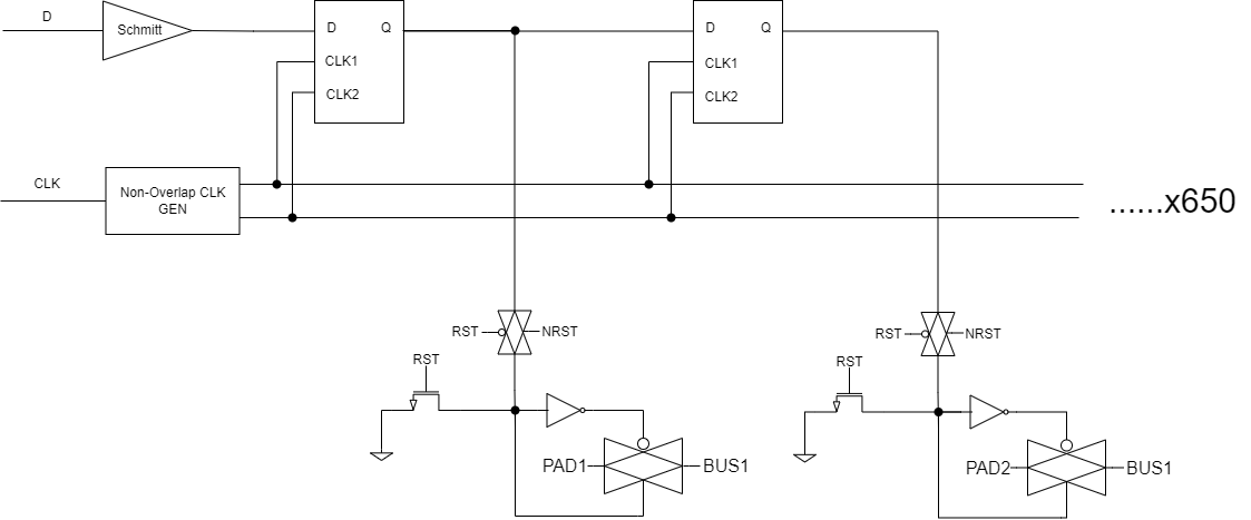
Fig. 10.1 Partial schematic of the 650-stage shift register#
<Labeling of the signals is not consistent; what is RST compared to EN? D needs to be DATA; RST is active-low so it must be inverse of EN>
The off-chip clock CLK is converted into two non-overlapping clock phases \(\phi\) and \(\overline{\phi}\) on chip to make sure that no hold-time violations occur in the register. A Schmitt Trigger is added to the DATA and EN line (not shown) to further improve the noise robustness of the signaling.
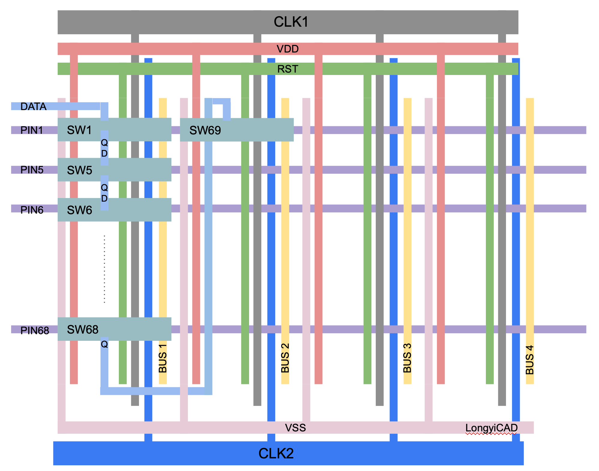
Fig. 10.2 Organization of the layout of a stage in the shift register#
<Add a timing diagram for the shift register>
10.2.3. Top-Level Layout#
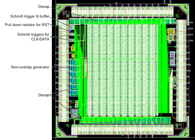
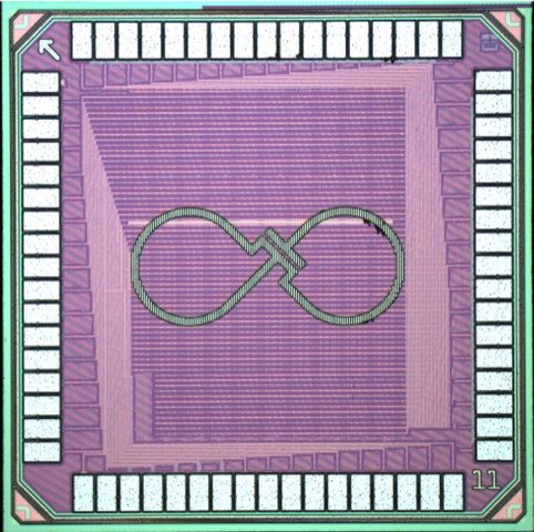
Fig. 10.3 Layout view of the 1mm x 1mm MOSbius chip#
The chip includes 424pF of nMOS decoupling capacitance between VDD and VSS
10.2.4. Package Pins to Shift-Register Mapping#
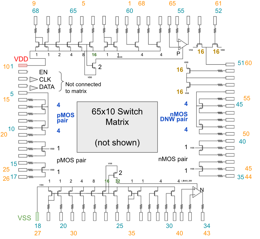
Fig. 10.4 Schematic of the MOSbius chip; blue pin numbers correspond to the numbering in the shift-register bitstream and the PCB labels, while orange numbers correspond to chip package pin numbers.#